Active organic light emitting diode (OLED)

An active, current technology, applied in the field of electronics, can solve the problems of multiple areas and affect the brightness of OLEDs, and achieve the effects of simple preparation methods, reducing opaque areas, and improving the brightness of OLEDs

Active Publication Date: 2013-01-16
NANJING CEC PANDA LCD TECH
View PDF7 Cites 9 Cited by
  • Summary
  • Abstract
  • Description
  • Claims
  • Application Information

AI Technical Summary

Problems solved by technology

The data line 1' and the current supply line 2' are respectively arranged on both sides of the organic light-emitting layer 7' so that the firs

Method used


Image

  • Active organic light emitting diode (OLED)
  • Active organic light emitting diode (OLED)
  • Active organic light emitting diode (OLED)

Examples


Embodiment 1

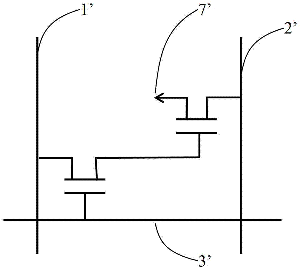
[0052] see figure 2 and image 3 As shown, the common electrode 4 and the scanning line 3 have the same layer structure.

[0053] The specific manufacturing steps are:

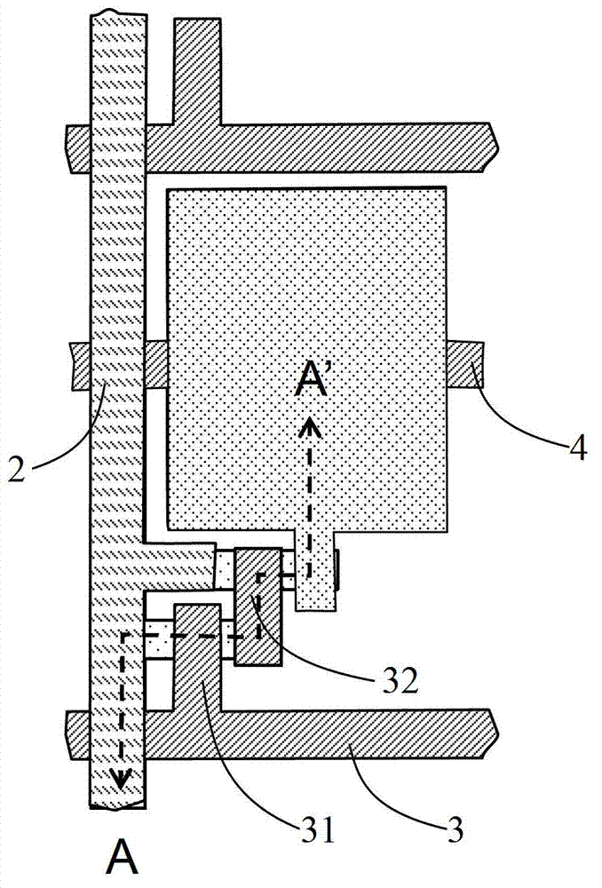
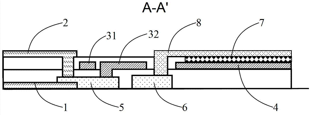
[0054] a. Please refer to Image 6 and Figure 7 As shown, the data line 1, the data TFT5 and the current TFT6 are first formed in sequence, and then the first insulating layer is formed, and the first contact hole 51 contacting the data TFT5 is opened on the first insulating layer; wherein, the current TFT5 and the data TFT6 The material is IGZO. IGZO (indium gallium zinc oxide) is the abbreviation of indium gallium zinc oxide. The amorphous IGZO material is the channel layer material used in the new generation of thin film transistor technology.

[0055] Wherein, the data TFT5 and the current TFT6 are located on the same side of the data line 1, the data TFT5 is connected to the data line 1, and the current TFT6 is separated from the data line 1; the current TFT6 is located on one side of the data TFT5...

Embodiment 2

[0060] see Figure 4 and Figure 5 As shown, the common electrode 4 and the data line 1 have the same layer structure.

[0061] The specific manufacturing steps are:

[0062] a. Please refer to Figure 14 and Figure 15 As shown, the data line 1, the common electrode 4, the current TFT6 and the data TFT5 are first formed in sequence, and then the first insulating layer is formed, and the data line 1, the two ends of the current TFT6 and the data TFT5 are opened on the first insulating layer. A contact hole with two ends in contact; wherein, the material of the current TFT6 and the data TFT5 is IGZO. IGZO (indium gallium zinc oxide) is the abbreviation of indium gallium zinc oxide. The amorphous IGZO material is the channel layer material used in the new generation of thin film transistor technology. Wherein, the current TFT6, the data TFT5 and the common electrode 4 are located on the same side of the data line 1 and are separated from the data line 1, wherein the data TF...


PUM


Abstract

The invention discloses an active organic light emitting diode (OLED), which comprises a data line, a power supply line, a scanning line, a common electrode, a data thin film transistor (TFT), a current TFT, an organic luminous layer and a transparent electrode layer, wherein the data TFT, the current TFT and the data line are formed in the same layer; the organic luminous layer is formed on the common electrode, and coats the transparent electrode layer; the data line and the power supply line are made of different-layer metals and are overlapped; and the common electrode and the data line or the scanning line are formed in the same layer. According to the active OLED, the data line and the power supply line are made of different-layer metals and configured at the same position, and by the framework, an opaque area occupied by metal wires can be decreased, and the area of the luminous layer can be effectively increased to improve the brightness of the OLED in a top emitting OLED framework or a bottom emitting OLED framework.

Description

technical field [0001] The invention belongs to the field of electronic technology, and in particular relates to an active OLED. Background technique [0002] OLED stands for Organic Light-Emitting Diode (Organic Light-Emitting Diode), also known as Organic Electroluminescence Display (OELD). Since 2003, this kind of display device has been widely used in MP3 players because of its lightness, lightness, power saving and other characteristics. For DC and mobile phones, which are also digital products, OLED display devices have only been shown in some exhibitions before. The engineering samples of the screen have not yet entered the stage of practical application. But OLED screen has many incomparable advantages of LCD. Organic light-emitting diode (Organic Light-Emitting Diode, OLED) has self-illumination at the same time, no backlight is needed, high contrast, thin thickness, wide viewing angle, fast response speed, can be used for flexible panels, wide operating temperatu...

Claims


Application Information

Patent Timeline
IPC IPC(8): H01L27/32G09G3/32H01L21/77G09G3/3225
Inventor 洪孟逸
Owner NANJING CEC PANDA LCD TECH
Why Eureka
Try Eureka