LGA and BGA repair process

A kind of process and peaceful technology, applied in the field of microelectronics, can solve the problems of difficult PCB board solder joint overlap, difficult scraper, device blocking, etc., and achieve the effect of improving repair rate, easy operation and cost reduction

Inactive Publication Date: 2013-01-16
NETRON SOFT-TECH ZHUHAI CO LTD
View PDF4 Cites 10 Cited by
  • Summary
  • Abstract
  • Description
  • Claims
  • Application Information

AI Technical Summary

Problems solved by technology

[0004] However, there are deficiencies in the existing technology. First, a set of silk screen molds and fixtures can only be used for devices of one size and shape. However, there will be various devices in actual production, so multiple sets of molds and fixtures are required. The cost is high, and manpower is required for maintenance. A special silk screen mold costs about 200 yuan, and it also needs to be equipped with special rework equipment. The cost of a rework equipment ranges from tens of thousands to hundreds of thousands, so for small-scale It is not a small burden for the company
In addition, when the device is small, such as 5mm × 5mm, it is difficult for the scraper of the silk screen to operate on the screen printing mold; and when the device is large, such as attached figure 1 As shown, the existing silk screen mold is difficult to completely coincide with the solder joints on the PCB, and it is easy to be blocked by surrounding devices

Method used


Image

  • LGA and BGA repair process
  • LGA and BGA repair process
  • LGA and BGA repair process

Examples


Embodiment Construction

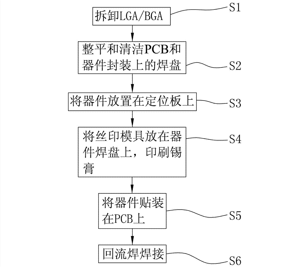
[0021] as attached figure 2 , attached image 3 As shown, the LGA and BGA rework process includes the following steps:

[0022] Step S1, remove the LGA / BGA from the PCB board, use hot air convection or a heating table to heat the device 4 package, when all the solder joints under the device 4 package are melted, use a vacuum nozzle or a Use tweezers to remove the device 4 package from the PCB.

[0023] Step S2, leveling and cleaning the pads on the PCB and the LGA / BGA package. After the device 4 is removed from the PCB, solder remains on the pads of the PCB and device 4. Use a solder suction gun to absorb the hot-melted solder Walk.

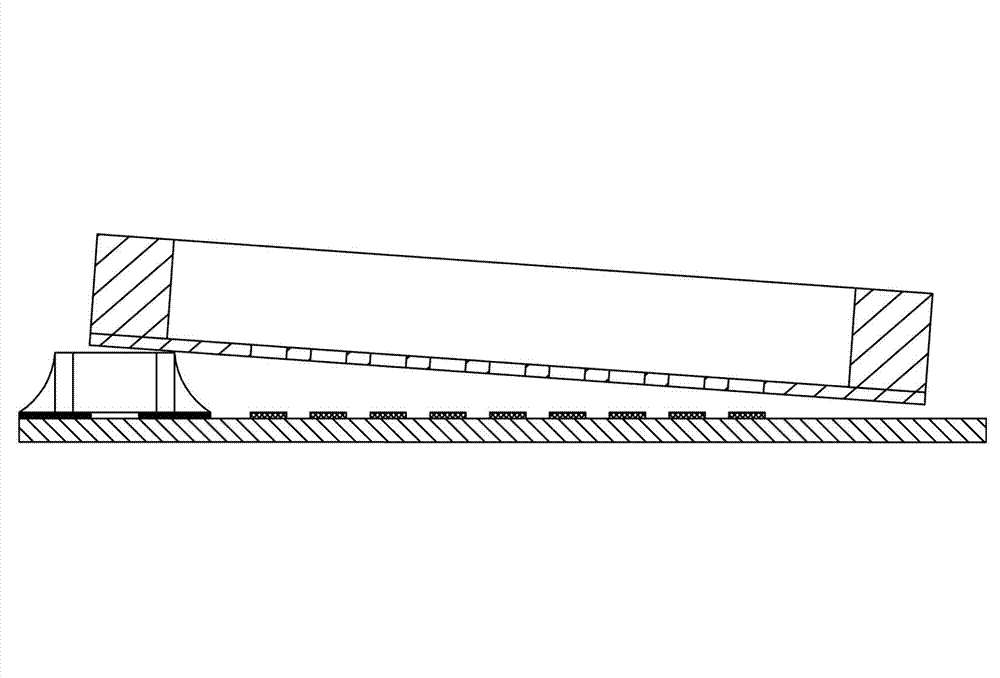
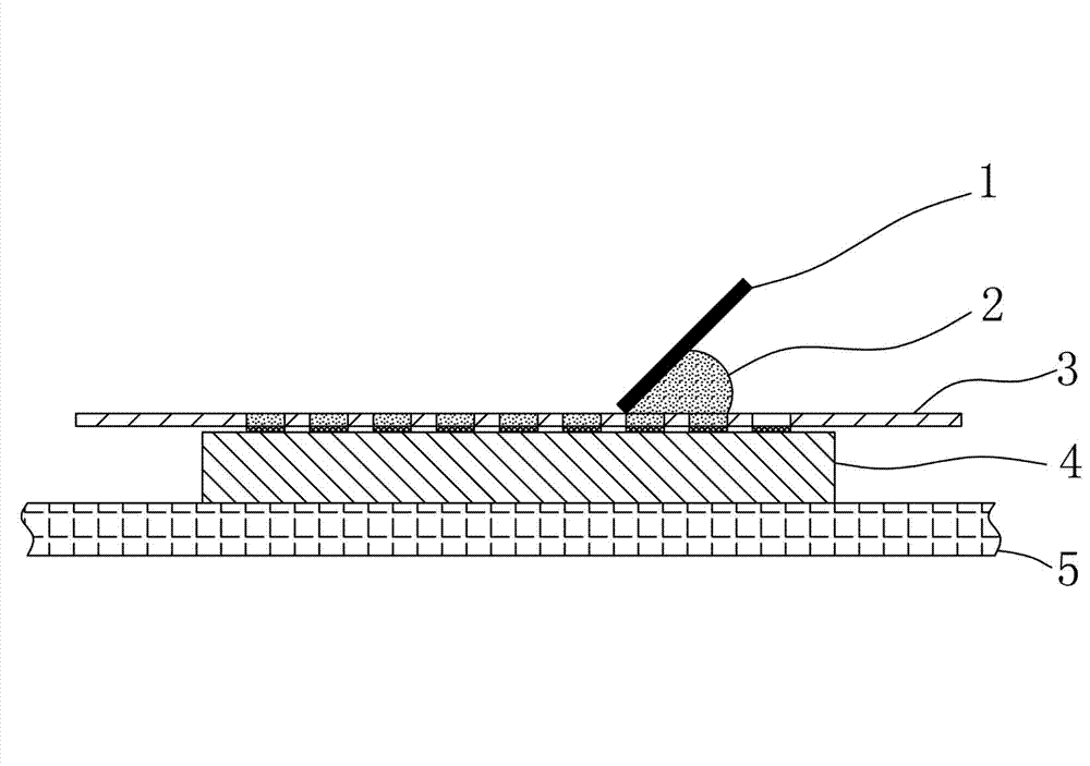
[0024] Step S3, placing the side of the LGA / BGA with solder joints facing up on the positioning plate 5, the positioning plate 5 is a silica gel plate, which has a certain viscosity, and the operator puts the back of the device 4 on the positioning plate 5 , and then lightly press the device 4 to stick the device 4 on the positioning board 5...


PUM


Abstract

The invention discloses an LGA (Land Grid Array) and BGA (Ball Grid Array) repair process and belongs to the technical field of microelectronics. By directly carrying out silk-screen printing on solder paste on a device and using a silk-screen printing die made of a FR4 material, the repair operation is simpler and more convenient, the waste is also reduced, the cost is reduced and the LGA and BGA repair process can be widely applied.

Description

technical field [0001] The invention relates to a LGA and BGA rework process, which belongs to the technical field of microelectronics. Background technique [0002] With the development and wide application of grid array packaging (hereinafter referred to as LGA) and ball grid array IC (hereinafter referred to as BGA) packaging, it will become the best choice for high-density, high-performance, and multi-functional packaging. Due to the special packaging forms of LGA and BGA, the solder joints are located at the bottom of the package body. If there is poor soldering, special rework equipment and corresponding processes are required for rework. [0003] The existing rework methods are described as follows: 1. Use hot air convection to heat the LGA / BGA package; 2. After all the solder joints under the LGA / BGA are melted, remove the LGA / BGA from the PCB ;3. Level and clean the pads on the PCB and LGA / BGA packages; 4. Print solder paste or solder paste on the PCB pads with a s...

Claims


Application Information

Patent Timeline
Patent Type & Authority Applications(China)
IPC IPC(8): H05K3/34B23K1/00
Inventor 黄清华
Owner NETRON SOFT-TECH ZHUHAI CO LTD
Why Eureka
Try Eureka