A kind of light-emitting diode laser etching method

A laser etching method and light-emitting diode technology, which are applied in laser welding equipment, electrical components, circuits, etc., can solve the problems of product yield impact, high cost, complex process, etc., to reduce product cost, reduce formation time, The effect of reducing the length of the process

Active Publication Date: 2017-05-10
WUXI CHINA RESOURCES HUAJING MICROELECTRONICS
View PDF12 Cites 0 Cited by
  • Summary
  • Abstract
  • Description
  • Claims
  • Application Information

AI Technical Summary

Problems solved by technology

However, due to the deep etching depth of the isolation trench of the integrated light emitting diode, the etching process time required by general etching equipment (such as ICP) is long, and in the etching process, the long process time will significantly reduce the efficiency of the ICP equipment. Therefore, the isolation trench etching of integrated light-emitting diodes using inductive plasma coupled etching has a negative impact on equipment, production capacity, and cost.
Moreover, ICP etching is the etching of the front side of the wafer, so a thicker (usually 0.5-2 microns in thickness) masking layer (such as SiO2) needs to be grown on the non-etching area before etching. 2 、Si 3 N 4 etc.) for protection, the process becomes complicated and the cost is high, and the quality of the masking layer will also have a great impact on the product yield

Method used


Image

  • A kind of light-emitting diode laser etching method
  • A kind of light-emitting diode laser etching method
  • A kind of light-emitting diode laser etching method

Examples


Embodiment Construction

[0031] The technical solutions of the present invention will be further described below in conjunction with the accompanying drawings and through specific implementation methods.

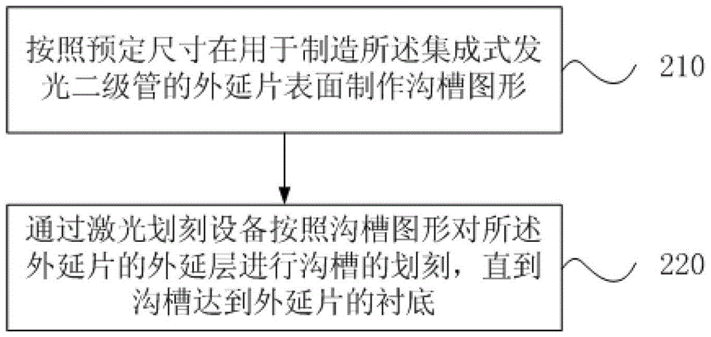
[0032] figure 2 It is a flow chart of the laser etching method for light-emitting diodes according to the first embodiment of the present invention. like figure 2 As shown, the method includes:

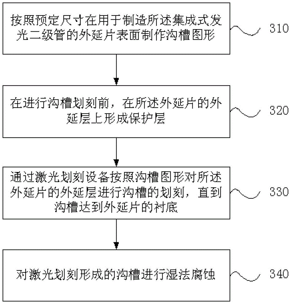
[0033] Step 210, making groove patterns on the surface of the epitaxial wafer used to manufacture the integrated light emitting diode according to predetermined dimensions.

[0034] Step 220, using laser scribing equipment to scribe grooves on the epitaxial layer of the epitaxial wafer according to the groove pattern until the groove reaches the substrate of the epitaxial wafer.

[0035] Wherein, the etching depth of the groove is controlled by controlling the marking speed and / or laser power of the laser marking equipment so that the marking depth reaches the substrate, and the marking speed and laser...


PUM


Abstract

The invention discloses a laser etching method for a light-emitting diode, which is used for etching an isolation groove for an integrated light-emitting diode. The method comprises the following steps: manufacturing a groove pattern on the surface of an epitaxial wafer used for manufacturing the integrated light-emitting diode according to the predetermined size; carrying out groove scribing to an epitaxial layer of the epitaxial wafer through a laser scribing device according to the groove pattern till the groove reaches the substrate of the epitaxial wafer; and forming a dielectric insulating layer in the groove. The invention further discloses a method for manufacturing an integrated light-emitting diode by using laser etching. The laser scribing device is used for etching the isolation groove for the integrated light-emitting diode, and a thick mask layer is not required, so that the formation time of the isolation groove is reduced, the process length is reduced, the yield of products is improved, and the product cost is greatly reduced.

Description

technical field [0001] The invention relates to semiconductor manufacturing technology, in particular to a laser etching method of a light emitting diode and a manufacturing method of an integrated light emitting diode. Background technique [0002] The integrated light-emitting diode realizes the metal interconnection between each light-emitting diode through the semiconductor process at the chip level, so that multiple light-emitting diodes can be connected in series or in parallel without using the PCB board, which simplifies the process and reduces the cost. Moreover, the performance of the integrated light-emitting diode is more stable, and it is widely used. [0003] figure 1 It is a schematic diagram of the structure of an integrated light-emitting diode chip. like figure 1 As shown, a plurality of light-emitting diode chips of an integrated light-emitting diode 10 are formed on a unified substrate 11 (such as a sapphire substrate), and each light-emitting diode ch...

Claims


Application Information

Patent Timeline
Patent Type & Authority Patents(China)
IPC IPC(8): H01L33/00B23K26/364B23K26/18
Inventor 王磊李国琪余志炎
Owner WUXI CHINA RESOURCES HUAJING MICROELECTRONICS
Why Eureka
Try Eureka