Test method for burr interference trigger chip latch-up effect
A latch-up effect and interference triggering technology, which is applied in the direction of electronic circuit testing, etc., can solve problems such as easy trigger latch-up effect and failure to meet the requirements of chip application testing.
- Summary
- Abstract
- Description
- Claims
- Application Information
AI Technical Summary
Problems solved by technology
Method used
Image
Examples
Embodiment Construction
[0019] The following example specifically illustrates the latch-up test process using one or more glitch pulse waves with a certain width as the test trigger waveform.
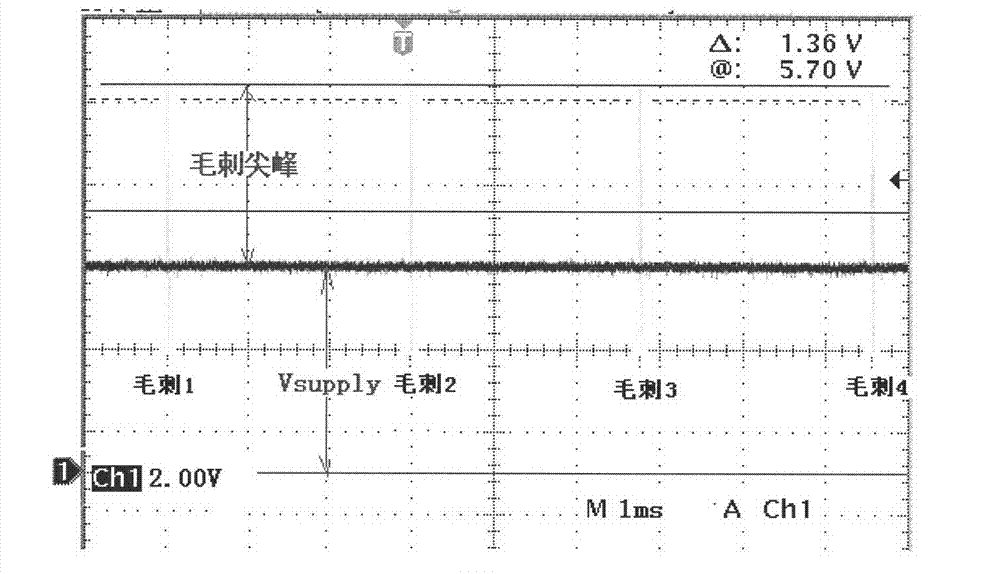
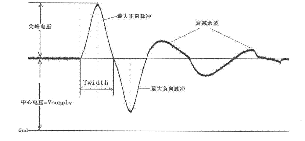
[0020] Such as figure 2 As shown, the number of glitches per unit time in multiple glitch pulse waves with a certain interval is called glitch density. For the maximum peak voltage value and maximum pulse width Twidth of a single glitch pulse wave, see image 3 .
[0021] Before the latch-up effect test is performed on the chip, the test range of the glitch density of the scheduled trigger glitch wave is 1 / 10ms to 10000 / 10ms, and the test range of the maximum peak voltage value of the scheduled trigger glitch wave is 7.5V to 127.5V. The maximum pulse width Twidth test range of the trigger glitch wave is 1ns~2.88μs. When the operating power supply voltage of the chip under test is 5V at most, set the center voltage of the trigger glitch wave of the damped oscillatory wave generator to 5V.
[0022] Set the g...
PUM
 Abstract
Description
Claims
Application Information
 - R&D
- Intellectual Property
- Life Sciences
- Materials
- Tech Scout
- Unparalleled Data Quality
- Higher Quality Content
- 60% Fewer Hallucinations
Browse by: Latest US Patents, China's latest patents, Technical Efficacy Thesaurus, Application Domain, Technology Topic, Popular Technical Reports.
© 2025 PatSnap. All rights reserved.Legal|Privacy policy|Modern Slavery Act Transparency Statement|Sitemap|About US| Contact US: help@patsnap.com


