
Polycrystalline silver platinum alloy plasma thin-film material and preparation method thereof
A technology of plasma and thin film materials, which is applied in metal material coating process, ion implantation plating, coating, etc., can solve the problems of complex preparation process, achieve low loss, adjustable dielectric function, and surface roughness small effect
- Summary
- Abstract
- Description
- Claims
- Application Information
AI Technical Summary
Problems solved by technology
Method used
Image

Examples
Embodiment 1
[0031] To clean the monocrystalline silicon substrate, put the pre-cut silicon wafer of 15 mm×8 mm into acetone for 8-10 minutes and ultrasonically clean it for 8-10 minutes, then put it in absolute ethanol for 8-10 minutes, and then place the The slices were put into ultrapure water and sonicated for 8-10 minutes. After immersing the cleaned substrate in 4% hydrofluoric acid for 20 seconds, take it out and dry it.
[0032] Put the cleaned substrate into the sputtering chamber, and place the prepared multiple silver-platinum alloy composite targets on the sputtering target position (according to different composition requirements, place different numbers of platinum sheets respectively).
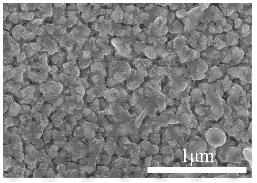
[0033] Ag was deposited on a silicon substrate by DC reactive magnetron sputtering 1-x Pt x Alloy thin film, use the imported vacuum molecular pump to pump the back vacuum to 1.5×10 -4 Pa. In the DC reactive magnetron sputtering deposition step, argon is the reactive sputtering gas, the...
Embodiment 2
[0037] As in Example 1, four platinum sheets and a silver target are used to form a composite target, and the silver-platinum alloy film is obtained according to the process in Example 1, and the composition of the film is Ag-25at%Pt alloy obtained by X-ray photoelectron spectroscopy analysis. film.
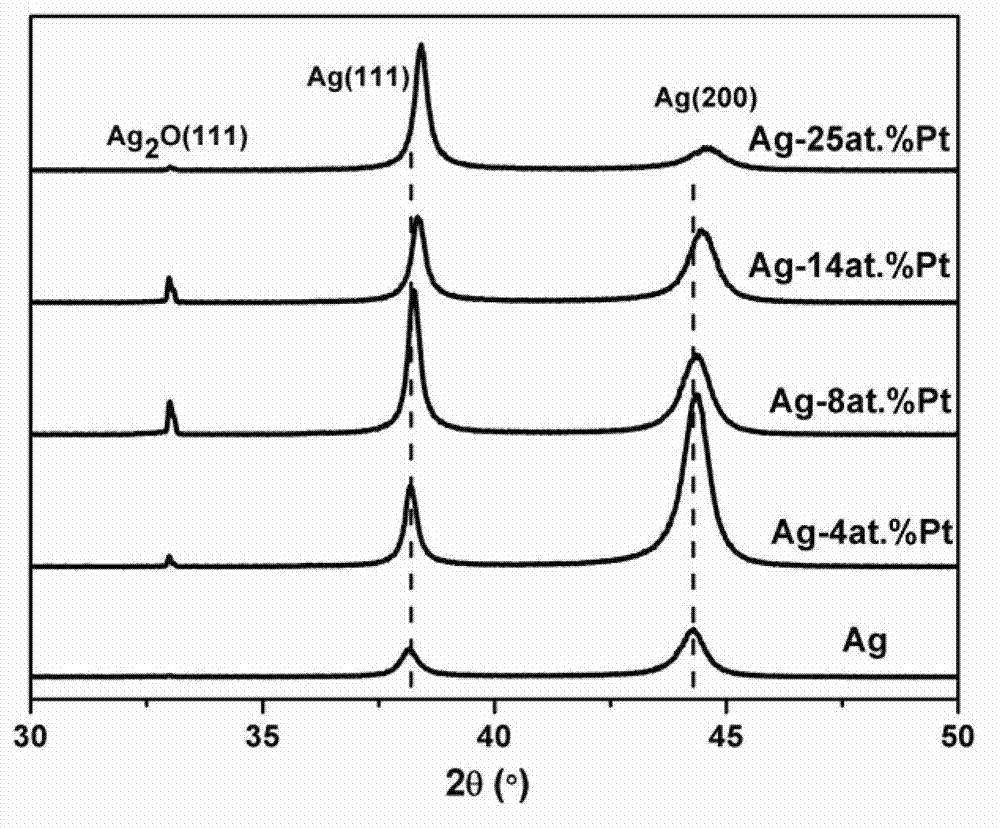
[0038] The tube furnace GSL-1500X-50 with argon protection function produced by Hefei Kejing Company was used for annealing, and the annealing temperatures were set at 100 °C, 200 °C and 300 °C, respectively. Utilize X-ray diffractometer to obtain the diffractogram (as Figure 4 As shown), the crystal phase and grain size distribution were analyzed, and the grain size in the obtained alloy film was dominated by Ag (200) orientation, and the average grain size was about 15 nm.
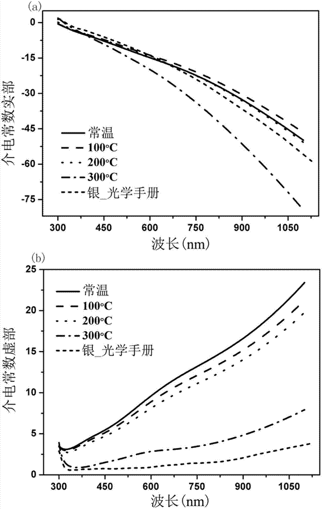
[0039] Utilize the ellipsometer produced by J.A. Woollam Company of the United States to measure the dielectric function of the Ag-25at%Pt alloy film after different annealing temperatures, such as Figu...
PUM
| Property | Measurement | Unit |
|---|---|---|
| thickness | aaaaa | aaaaa |
| thickness | aaaaa | aaaaa |
| thickness | aaaaa | aaaaa |
Abstract
Description
Claims
Application Information