Graphical transport layer, organic light-emitting diode(OLED) device containing graphical transport layer and preparation method

A transmission layer and patterning technology, applied in semiconductor/solid-state device manufacturing, electric solid-state devices, semiconductor devices, etc., can solve the problems of loss of effective light-emitting area, complex structure, and reduced luminous intensity of OLED devices, so as to improve light output efficiency , The effect of maximizing the luminous area

Active Publication Date: 2013-03-13
GUAN YEOLIGHT TECH CO LTD +1
View PDF5 Cites 6 Cited by
  • Summary
  • Abstract
  • Description
  • Claims
  • Application Information

AI Technical Summary

Problems solved by technology

[0004] The technical problem to be solved by the present invention is that in the existing scheme, the structure is relatively complicated, the preparation process is special, and the OLED device loses the effective light-emitting area while improving the light output coupling efficiency, resulting in a decrease in the luminous intensity of the OLED device. Patterned transmission layer that improves light output coupling efficiency while not affecting light emitting area of ​​OLED device, OLED device with the patterned transmission layer and preparation method thereof

Method used


Image

  • Graphical transport layer, organic light-emitting diode(OLED) device containing graphical transport layer and preparation method
  • Graphical transport layer, organic light-emitting diode(OLED) device containing graphical transport layer and preparation method
  • Graphical transport layer, organic light-emitting diode(OLED) device containing graphical transport layer and preparation method

Examples


Embodiment 1

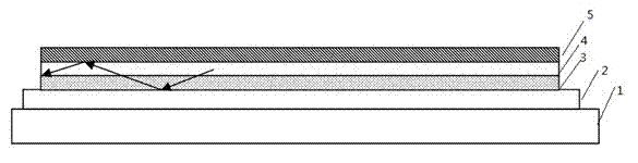
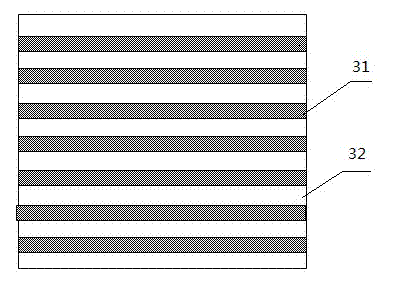
[0062] This embodiment provides a patterned transmission layer, the patterned transmission layer includes a conductive high-refractive-index region and a conductive low-refractive-index region, and the difference in refractive index between the high-refractive-index region and the low-refractive-index region is Value > 0.2. As a preferred implementation manner, the difference in refractive index between the high refraction region and the low refraction region can be selected to be >0.3. As a possible implementation manner, the refractive index of the high refractive index region is between 1.8-3.0; the refractive index of the low refractive index region is between 1.6-2.3.

[0063] In this embodiment, the high refractive index region is made of high refractive index material NPB with a refractive index of 1.8; the low refractive index region is made of NPB with a refractive index of 1.8 and MgF with a refractive index of 1.3. 2 Prepared by mixing, wherein NPB with a refractiv...

Embodiment 2

[0069] The OLED device in this embodiment has the same structure as the OLED device in Embodiment 1;

[0070] The preparation method is also the same, except that when preparing the patterned transmission layer, the low refractive index region uses NPB with a refractive index of 1.8 and MgF with a refractive index of 1.3. 2 Prepared by mixing, wherein NPB with a refractive index of 1.8 accounts for 70 parts by weight, and MgF with a refractive index of 1.3 2 Accounting for 30 parts by weight.

Embodiment 3

[0072]The OLED device in this embodiment has the same structure as the OLED device in Embodiment 1;

[0073] The preparation method is also the same, except that when preparing the patterned transmission layer, the low refractive index region uses NPB with a refractive index of 1.8 and MgF with a refractive index of 1.3. 2 Prepared by mixing, wherein NPB with a refractive index of 1.8 accounts for 50 parts by weight, and MgF with a refractive index of 1.3 2 Accounting for 50 parts by weight.


PUM


Abstract

The invention discloses a graphical transport layer, an organic light-emitting diode(OLED) device containing the graphical transport layer and a preparation method. The graphical transport layer comprises a conductive high refractive index region and a conductive low refractive index region, wherein the difference of refractive indexes of the high refractive index region and the low refractive index region is more than 0.2, the graphical transport layer is arranged between a first electrode and an organic electroluminescence layer of the OLED device, the total light reflection quantity of the OLED device can be reduced effectively, the light extraction efficiency of the OLED device is improved, and the method is easy to implement and integrate and obvious in effect.

Description

technical field [0001] The invention relates to an organic electroluminescent device, in particular to a patterned transport layer, an OLED device comprising the patterned transport layer and a preparation method. Background technique [0002] OLED (Organic Light-Emitting Diode) is an organic light-emitting diode. As a display device, it has the advantages of wide viewing angle, fast response, and wide color gamut. As a lighting device, it has the characteristics of planarization, no mercury pollution, and high efficiency. It is the next generation Display and lighting trends. In a typical OLED device structure, due to the total reflection caused by the inconsistency of the refractive index of each layer material, most of the light emitted through the emitting layer of the OLED device is confined in the device and cannot be effectively output to the outside of the device, that is, the optical coupling efficiency is low. [0003] Methods to improve light extraction efficienc...

Claims


Application Information

Patent Timeline
Patent Type & Authority Applications(China)
IPC IPC(8): H01L51/50H01L51/52H01L51/56
Inventor 邱勇段炼张国辉王静董艳波
Owner GUAN YEOLIGHT TECH CO LTD
Why Eureka
Try Eureka