Organic el display, method of producing organic el display, and electronic unit

A manufacturing method and display technology, which can be applied to the manufacturing of organic semiconductor devices, semiconductor/solid-state devices, circuits, etc., can solve the problems of reduced light extraction efficiency and reduced image visibility, so as to suppress external light reflection, achieve miniaturization, high the effect of clarity

Active Publication Date: 2013-03-13
SONY CORP
View PDF6 Cites 15 Cited by
  • Summary
  • Abstract
  • Description
  • Claims
  • Application Information

AI Technical Summary

Problems solved by technology

However, when the thickness is increased, the light extraction efficiency decreases due to the absorption of light in the cathode electrode
This leads to disadvantages such as decreased visibility of the displayed image

Method used


Image

  • Organic el display, method of producing organic el display, and electronic unit
  • Organic el display, method of producing organic el display, and electronic unit
  • Organic el display, method of producing organic el display, and electronic unit

Examples


no. 1 example

[0051] 1. Structure

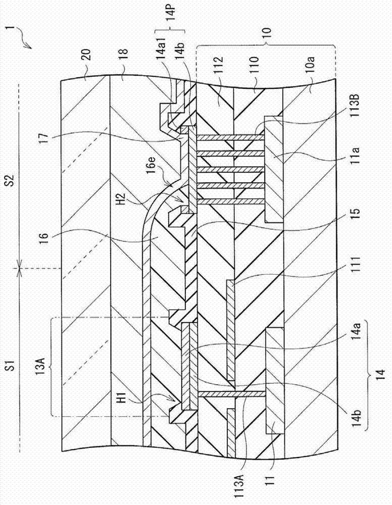
[0052] figure 1 The sectional configuration of the organic EL display (organic EL display 1 ) according to the first embodiment of the present invention is illustrated. The organic EL display 1 is, for example, a so-called top emission type. In the organic electroluminescent display 1 , for example, a plurality of organic electroluminescent devices (EL device sections 13A) are arranged in a matrix in a display region S1 on a drive substrate 10 . It should be noted that figure 1 One of these EL device portions 13A and an electrode pad 14P to be described later (in the vicinity of the boundary between the display region S1 and the peripheral region S2 ) are illustrated. Each of the EL device sections 13A is formed with, for example, any one of a red (R) sub-pixel, a green (G) sub-pixel, and a blue (B) sub-pixel, and such three sub-pixels function as one pixel. effect.

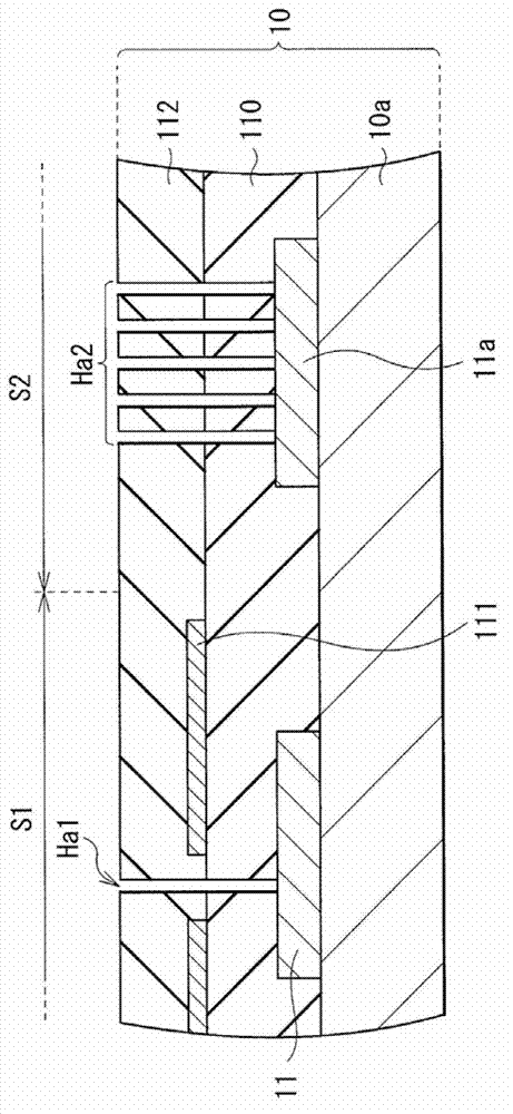
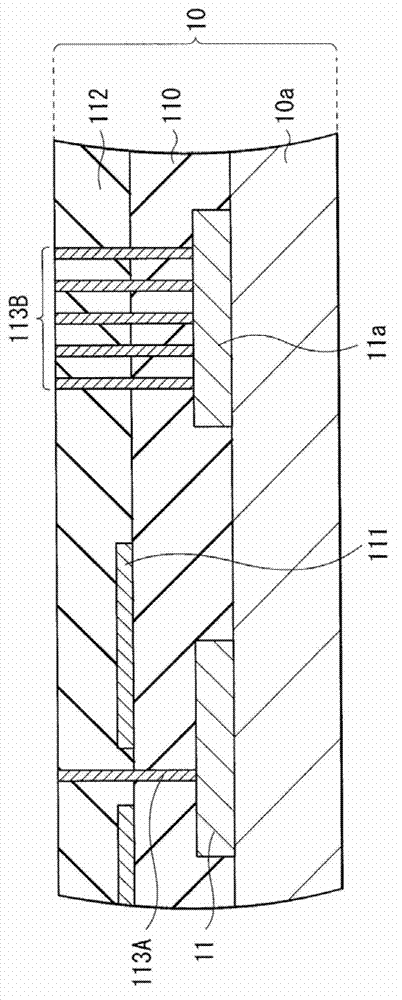
[0053] Drive substrate 10

[0054] In the drive substrate 10 , a drive circuit (pi...


PUM


Abstract

An organic EL display includes: a plurality of first electrodes provided in a display region on a drive substrate, the plurality of first electrodes each including a laminated film having two or more layers; an organic layer provided on the plurality of first electrodes and including a light emitting layer; an electrode pad provided in a peripheral region around the display region; and a second electrode provided on the organic layer as well as the electrode pad, wherein the laminated film includes a first conductive film functioning as a reflective film, and a second conductive film provided below the first conductive film, and having a reflectance lower than that of the first conductive film, and the electrode pad corresponds to a part of the laminated film, and includes a conductive film made of a material same as that of the second conductive film.

Description

[0001] Cross References to Related Applications [0002] This application contains subject matter related to that disclosed in Japanese Priority Patent Application JP 2011-191035 filed with Japan Patent Office on Sep. 1, 2011, the entire content of which is hereby incorporated by reference in its entirety. into this article. technical field [0003] The present invention relates to an organic EL display that displays an image by utilizing an organic electroluminescence (EL) phenomenon of an organic material, a method for manufacturing the organic EL display, and an electronic device including the organic EL display. Background technique [0004] A top emission type organic EL display has a device structure in which an organic EL layer is interposed between a lower electrode (for example, an anode electrode) and an upper electrode (for example, a cathode electrode). The lower electrode functions as a reflective electrode. In this device structure, light is taken out from th...

Claims


Application Information

Patent Timeline
Patent Type & Authority Applications(China)
IPC IPC(8): H01L51/52H01L27/32H01L51/56
CPCH01L51/5221H01L27/3276H01L2251/5315H01L51/5218H10K59/131H10K50/818H10K50/828H10K2102/3026
Inventor 长谷川英史槙田笃哉山田二郎横山诚一野田英利佐川裕志
Owner SONY CORP
Why Eureka
Try Eureka