Method for fixing printed circuit board (PCB) with mark point location function

A PCB board and point positioning technology, which is applied to the assembly of printed circuits with electrical components, auxiliary devices, auxiliary welding equipment, etc., can solve the problem of PCB board position deviation, poor soldering effect, affecting the practicability and operating efficiency of automatic soldering robots, etc. problems, achieve the effect of reducing welding time and increasing welding speed

Active Publication Date: 2013-03-20
廖怀宝
View PDF4 Cites 37 Cited by
  • Summary
  • Abstract
  • Description
  • Claims
  • Application Information

AI Technical Summary

Problems solved by technology

Every time the PCB board is fixed, the on-site operators manually adjust and fix the PCB board to the same position. However, due to the differences in the proficiency, strength, etc. When clamping and fixing, it will cause different deformation or rotation of the PCB, which will lead to deviations in the position of a series of PCB boards corresponding to the same program file, which will lead to poor soldering effect or even inability to solder, and ultimately affect the practicality of the automatic soldering robot sex and work efficiency

Method used


Image

  • Method for fixing printed circuit board (PCB) with mark point location function
  • Method for fixing printed circuit board (PCB) with mark point location function
  • Method for fixing printed circuit board (PCB) with mark point location function

Examples


Embodiment Construction

[0050] The present invention will be described in detail below in conjunction with the accompanying drawings.

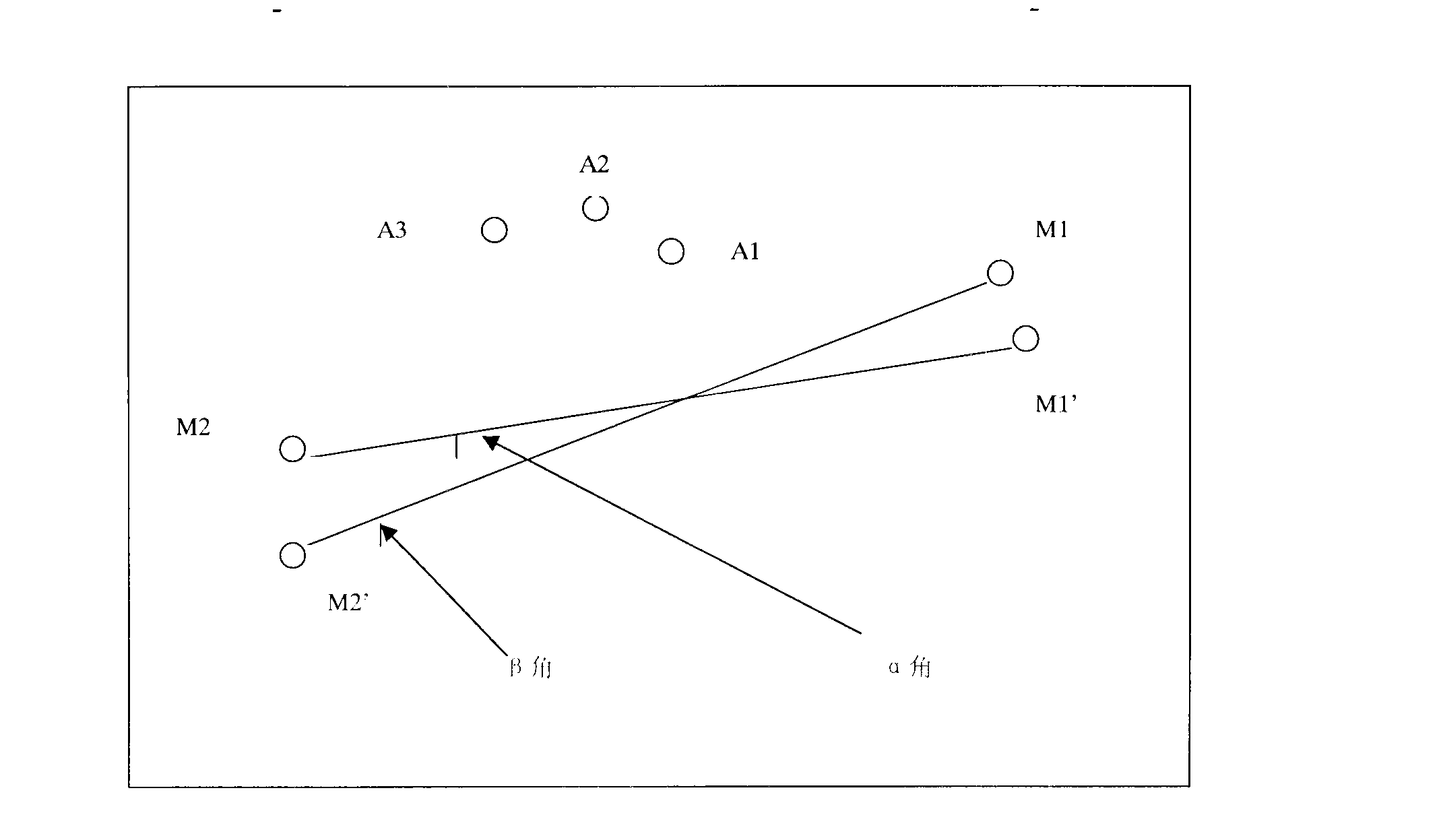
[0051] Such as figure 1 As shown, the Mark point is already done in the PCB board design stage. It is the position identification point where the PCB is applied to the automatic placement machine in the circuit board design. It is also called a mark point or a feature point. Points are generally circular markers. However, offsets often occur when the PCB board is placed. The present invention introduces the positioning function of the Mark point into the automatic soldering robot to fix the PCB board.

[0052] The general approach is:

[0053] 1. When doing the program, first place a reference PCB board on the fixture, take a picture of the Mark point on the PCB board with the camera, and display it on the computer screen, and then use the screenshot control that comes with the solder robot software on the Capture the image of the Mark point area in the current fi...


PUM


Abstract

Disclosed is a method for fixing a printed circuit board (PCB) with a mark point location function. The method is characterized by including the following steps: (1) firstly obtaining two mark point images on a reference PCB with a camera when programs are made, (2) obtaining two mark point images which are matched with two chosen mark point positions in the programming process and are on the detected PCB with the camera in the process of welding, and (3) comparing two groups of mark points which are captured in the step (1) and the step (2). If the two groups of the mark points are not out of position, the board position is normal, and if skewing exists, the PCB can be compensated. By the means of the method for fixing the PCB with the mark point location function, welding precision can not be influenced by the factors such as the size, the height and the skewing of the PCB, and simultaneously, welding time is deceased and welding speed is increased.

Description

technical field [0001] The invention relates to the technical field of automatic soldering robots, in particular to a method for adding a PCB board mark point auxiliary positioning function to an automatic soldering robot, so that the same batch of different PCB boards can effectively improve the soldering points of the same batch of PCB boards when performing PCB soldering operations positioning accuracy. Background technique [0002] Automatic soldering robot is an automation system widely used in major factories and enterprises in China. It has the characteristics of stable performance, large working space, fast movement speed and strong load capacity. The welding quality is obviously better than manual welding, which greatly improves the welding operation. production efficiency. Its appearance will greatly reduce production costs and transform manual work into automatic operation of machines. Users can also adjust various parameters of the robot according to different ...

Claims


Application Information

Patent Timeline
Patent Type & Authority Applications(China)
IPC IPC(8): B23K37/04B23K1/00H05K3/34
Inventor 廖怀宝
Owner 廖怀宝
Why Eureka
Try Eureka