Integrated circuit defect optical detection method and device

An integrated circuit, optical detection technology, applied in the direction of measuring devices, optics, optical components, etc., can solve the problems of enhancement, increase the error rate of defect detection, etc., and achieve the effect of high defect detection accuracy

Active Publication Date: 2013-04-03
SKYVERSE TECH CO LTD
View PDF10 Cites 5 Cited by
  • Summary
  • Abstract
  • Description
  • Claims
  • Application Information

AI Technical Summary

Problems solved by technology

Therefore, any selected phase difference between the reflected light and the reference light has the potential to enhance a part of the noisy signal
It can be seen that such a method will increase the error rate of defect detection

Method used


Image

  • Integrated circuit defect optical detection method and device
  • Integrated circuit defect optical detection method and device
  • Integrated circuit defect optical detection method and device

Examples


Embodiment Construction

[0039]The technical solutions in the embodiments of the present invention will be clearly and completely described below in conjunction with the accompanying drawings in the embodiments of the present invention. Obviously, the described embodiments are only some of the embodiments of the present invention, not all of them. Based on the embodiments of the present invention, all other embodiments obtained by persons of ordinary skill in the art without making creative efforts belong to the protection scope of the present invention.

[0040] In integrated circuits, circuit defects can affect or even destroy the normal function of the chip, directly leading to the failure of the device function. Therefore, the detection of defects in integrated circuits is very important in the manufacturing process of integrated circuits.

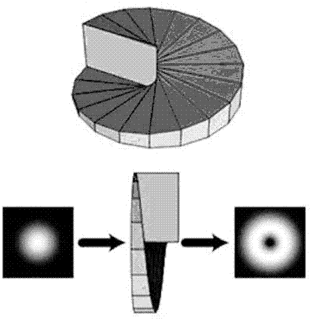
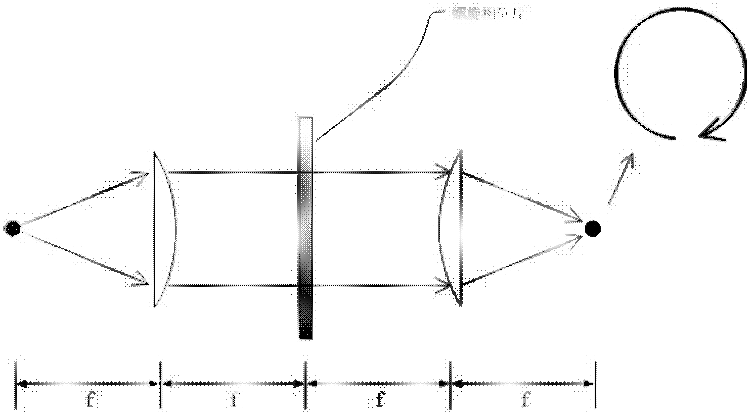
[0041] In the embodiment of the present invention, the spiral phase technology is applied to the detection of integrated circuit defects, and a spiral phase p...


PUM

PropertyMeasurementUnit
wavelengthaaaaaaaaaa

Abstract

The embodiment of the invention discloses an integrated circuit defect optical detection method and an integrated circuit defect optical detection device. The method comprises the steps that: a spiral phase plate is arranged at a Fourier plane; through the spiral phase plate, scattered light and reflected light of the defect on the integrated circuit are received, wherein the scattered light passes through the spiral phase plate and forms a circle image on an image receiving plane, and the reflected light passes through the center of the spiral phase plate and forms same-phase uniform background light on the image receiving plane; the circle image and the same-phase uniform background light are subjected to phase interference on the image receiving plane, such that a spot image comprising bright spots and dark spots is formed; and the type of defect on the integrated circuit is determined according to the spot image. According to the embodiment of the invention, integrated circuit defect detection precision can be improved.

Description

technical field [0001] The invention relates to the field of integrated circuit manufacturing, in particular to an optical detection method and device for defects in integrated circuits. Background technique [0002] Circuit defects exist in any semiconductor manufacturing process and are the main problem to be faced in the process development process before mass production. Defects not only come from random defects caused by pollution components in the environment during chip production, but also from system defects caused by imperfect processes. [0003] As the foundation and core of the electronics industry, the design process of the integrated circuit industry will enter the technology generation of 22nm and below. Therefore, how to continuously improve the manufacturing process in the research and development process and control the circuit defects that appear in the manufacturing process to at least 22 nanometers and below is the key to the success of the process. ...

Claims


Application Information

Patent Timeline
Patent Type & Authority Applications(China)
IPC IPC(8): G01N21/45G01N21/956
CPCG01N21/47G01N21/55G01N21/956G02B27/50
Inventor 陈鲁
Owner SKYVERSE TECH CO LTD
Why Eureka
Try Eureka