System and method for improving TFT-array manufacturing yields

a technology of tft-array and manufacturing yield, which is applied in the field of lcd manufacturing, can solve the problems of abnormally high number of reported defects, difficult identification of process non-uniformities and process contamination, and inability to repair tft-array repair equipmen

Inactive Publication Date: 2006-04-04
YIELDBOOST TECH
View PDF2 Cites 4 Cited by
  • Summary
  • Abstract
  • Description
  • Claims
  • Application Information

AI Technical Summary

Benefits of technology

[0013]An object of the invention is to solve at least the above problems and / or disadvantages and to provide at least the advantages described hereinafter.

Problems solved by technology

In most cases, defects caused by process non-uniformities and process contamination are hard to identify under a microscope, and they cannot be repaired by TFT-array repair equipment even if they are identified.
Inaccuracies in the TFT-array testing system can also cause an abnormally high number of reported defects.
In this case, reducing the number of reported defects to a number equal to or less than the predetermined critical number will result in the TFT-array testing system reporting a smaller number of potential defects, with the potential defects that are reported having a higher probability of being real defects.

Method used


Image

  • System and method for improving TFT-array manufacturing yields
  • System and method for improving TFT-array manufacturing yields
  • System and method for improving TFT-array manufacturing yields

Examples


Embodiment Construction

I. Thin-Film Transistor (TFT) Liquid Crystal Display (LCD) Fabrication

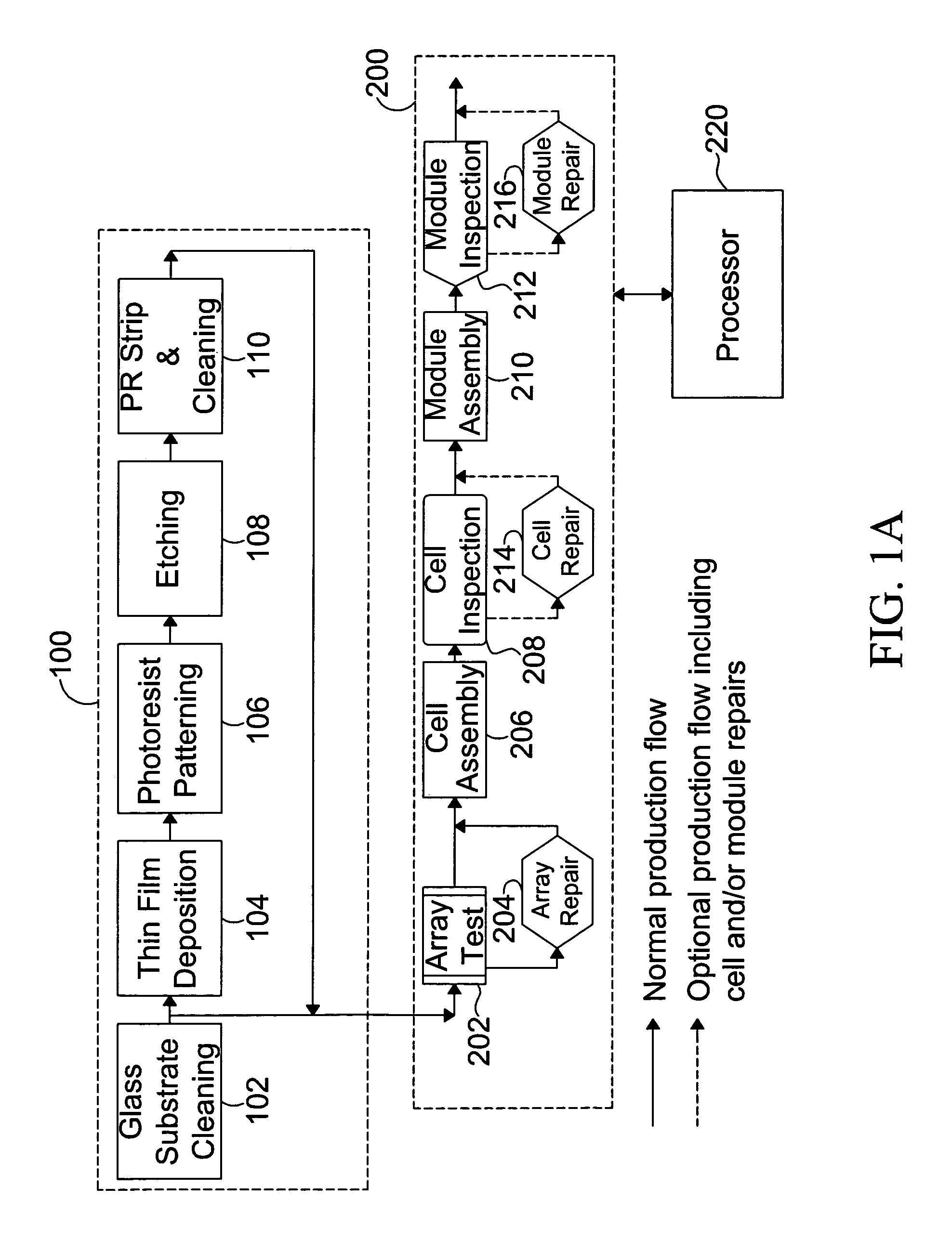
[0029]FIG. 1A is a block diagram of the process flow for TFT-LCD fabrication. The fabrication process can be divided into two stages, an array panel fabrication stage 100, in which the thin-film transistor (TFT) array panels are fabricated on a substrate, and a test and assembly stage 200, in which the TFT-array panels are tested and the displays are assembled.

[0030]In the array panel fabrication stage, the glass substrate on which the TFT-array panels are fabricated is cleaned at step 102. Steps 104–110 represent well known process steps for forming TFT-array panels on a glass substrate. They consist of a thin film deposition step 104, a photoresist patterning step 106, and etching step 108 and a photoresist stripping and cleaning step 110. Steps 104–110 are repeated for each patterned thin film layer that is deposited on the glass substrate.

[0031]Multiple TFT-array panels are typically fabricated on each glass s...


PUM


Abstract

A system and method for detecting defects in TFT-array panels is provided that improves defect detection accuracy by adjusting the thresholding parameters used to classify defective pixels when the number of defects reported by a TFT-array testing system exceeds a predetermined critical number. In a preferred embodiment, the thresholding parameters are adjusted until the number of reported defects is less than or equal to the predetermined critical number. The predetermined critical number represents a threshold number for determining if the number of reported defects is abnormally high. Reducing the number of reported defects to a number equal to or less than the predetermined critical number will decrease the operation time of the TFT-array repair equipment, because of the reduced number of potential defects it will be required to handle, and will also result in the TFT-array testing system reporting a smaller number of potential defects, with the potential defects that are reported having a higher probability of being real defects.

Description

CROSS-REFERENCE TO RELATED APPLICATIONS[0001]This application is a continuation-in-part of U.S. patent application Ser. No. 10 / 388,481, filed Mar. 17, 2003, which is a continuation-in-part of U.S. patent application Ser. No. 10 / 355,059, filed Jan. 31, 2003 now U.S. Pat. No. 6,862,489. The contents of both of the above-identifed U.S. Patent Applications are incorporated herein by reference in their entirety.BACKGROUND OF THE INVENTION[0002]1. Field of the Invention[0003]This invention relates to LCD manufacturing and, more particularly, to a system and method for improving TFT-array manufacturing yields.[0004]2. Background of the Related Art[0005]Yield management is important in LCD manufacturing. In LCD manufacturing, a single large plate of glass is divided into just a handful of LCD panels. As consumer demand grows for larger and larger displays, substrates get larger and the number of LCD panels per glass plate decreases. Accordingly, production yields are critical in LCD manufac...

Claims


Application Information

Patent Timeline
Patent Type & Authority Patents(United States)
IPC IPC(8): G01N27/00G01N35/00G06F19/00G01V3/00G02FG02F1/13G02F1/136G05B19/418
CPCG05B19/41875Y02P90/02G02F1/13G05B19/418
Inventor CHUNG, KYO YOUNG
Owner YIELDBOOST TECH
Why Eureka
Try Eureka