Semiconductor product detecting machine and detecting method thereof

A detection method and technology for semiconductors, which can be used in semiconductor/solid-state device testing/measurement, measurement devices, optical testing flaws/defects, etc., and can solve problems such as poor accuracy and low efficiency

Active Publication Date: 2013-04-03
ASE (KUNSHAN) INC
View PDF5 Cites 49 Cited by
  • Summary
  • Abstract
  • Description
  • Claims
  • Application Information

AI Technical Summary

Problems solved by technology

The semiconductor product inspection machine of the present invention solves the problems of low efficiency and poor accuracy caused by manual optical inspection, and can effectively avoid human-made operations or judgment errors when manual marking or laser engraving on the defective or inferior products , It can also prevent defective products (defective or inferior products) from being mixed with good products, thereby improving the quality of semiconductor products

Method used


Image

  • Semiconductor product detecting machine and detecting method thereof
  • Semiconductor product detecting machine and detecting method thereof
  • Semiconductor product detecting machine and detecting method thereof

Examples


Embodiment Construction

[0013] In order to make the above-mentioned purposes, features and advantages of the present invention more obvious and understandable, the preferred embodiments of the present invention will be specifically cited below, together with the accompanying drawings, for a detailed description as follows:

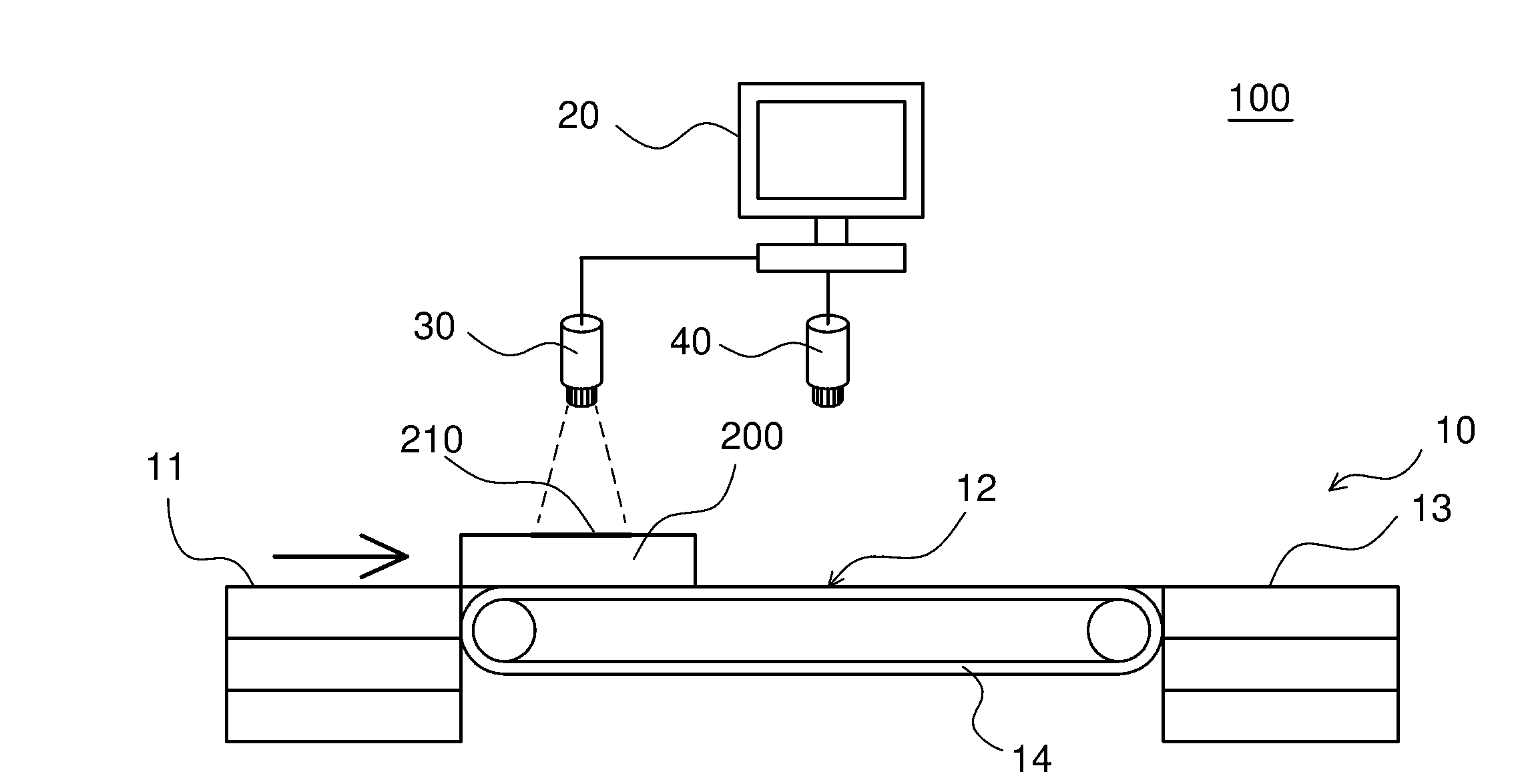
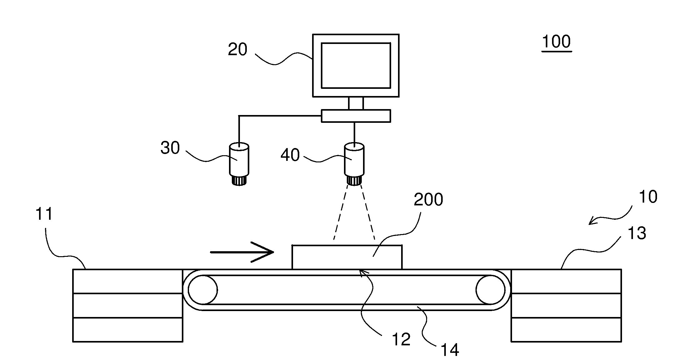
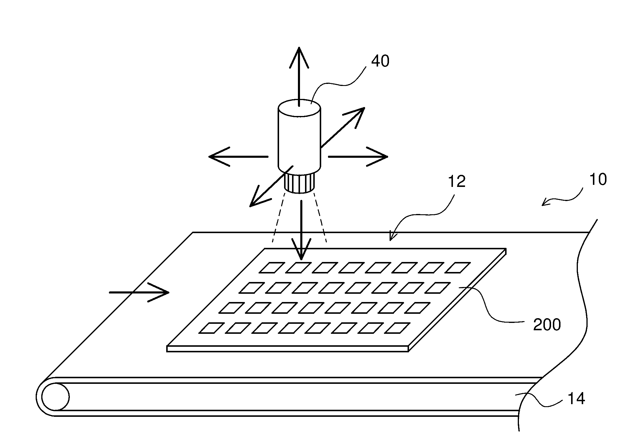
[0014] Please refer to Figures 1A to 1B , Figures 1A to 1B It is a schematic diagram of the operation of a semiconductor product inspection machine according to an embodiment of the present invention. A semiconductor product inspection machine 100 includes a work station 10 , a computer unit 20 , an identification camera 30 and at least one inspection camera 40 . Described work station platform 10 is provided with a feeding end 11, a working area 12, a feeding end 13 and a conveying device 14, and described conveying device 14 is used for a semiconductor product bar 200 to be tested (has several semiconductor products to be tested) Products) are transported from the loading end...


PUM


Abstract

The invention discloses a semiconductor product detecting machine and a detecting method thereof. The semiconductor product detecting machine comprises a working platform, a computer unit, an identification camera and at least one detection camera, wherein the identification camera identifies an identification code on a semiconductor product strip, and invokes a corresponding mapping image electronic document out, and the at least one detection camera intercepts an image of the semiconductor product, then performs a comparison detection task by comparing the image of the semiconductor product with an image comparison file, and records a detection result in a mapping image electronic document corresponding to the computer unit. The semiconductor product detecting machine not only can achieve automatic optic inspection and prevent man-made operation errors or judgment errors when a defect product (a non-performing product or a sub-quality product) is marked by a human or lasers, but also can prevent the defect product (the non-performing product or the sub-quality product) from mixing with good products, and therefore quality of the semiconductor product is improved.

Description

technical field [0001] The invention relates to a semiconductor product inspection machine and a detection method thereof, in particular to a semiconductor product inspection machine capable of automatically judging and recording the position of defective products (defective products or inferior products) and a detection method thereof. Background technique [0002] Nowadays, in order to meet the needs of various high-density packaging, the semiconductor packaging industry has gradually developed various types of packaging designs. Among them, the commonly used packaging carrier includes a packaging substrate with a multi-layer printed circuit and a metal substrate. A leadframe that is stamped or etched from a board. [0003] In the existing semiconductor packaging process using a lead frame as a package carrier, it mainly includes the following steps: first prepare a lead frame strip (leadframe strip), which has several lead frame units and a frame; The chips are correspon...

Claims


Application Information

Patent Timeline
Patent Type & Authority Applications(China)
IPC IPC(8): H01L21/66G01N21/89G01B11/00
Inventor 魏冬张建华李震宇吕松霖陈安利李磊
Owner ASE (KUNSHAN) INC
Why Eureka
Try Eureka