

Inspection jig and contact
A technology for inspecting fixtures and contacts, which is applied to electronic circuit testing, instruments, and electrical measurement, can solve problems such as complex processing and rising production costs, and achieve the effects of simplified structure, easy design, and shortened construction period
- Summary
- Abstract
- Description
- Claims
- Application Information
AI Technical Summary
Problems solved by technology
Method used
Image

Examples
Embodiment approach 1)
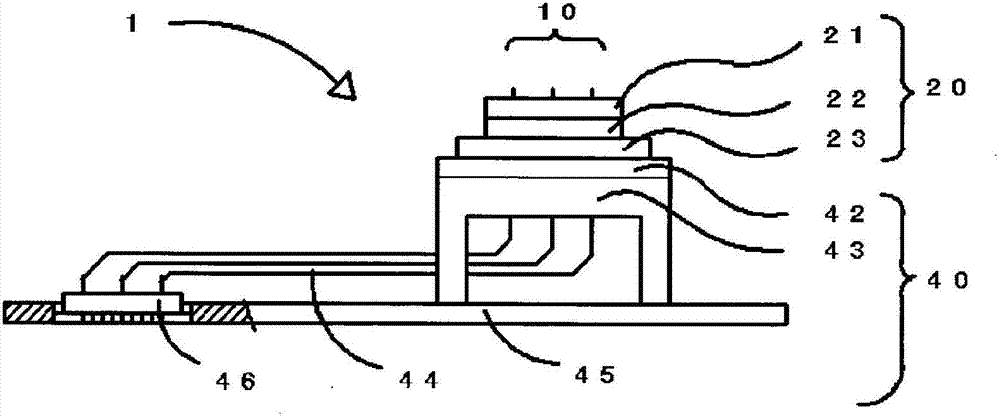
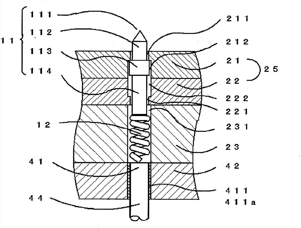
[0072] Such as figure 1 As shown, in the inspection jig 1 according to the embodiment of the present invention, a plurality of contacts 10 are held by the contact holder 20 and are detachably attached to the electrode plate 42 . figure 2 The electrode 41 shown is arranged coaxially with the coil spring 12 of the contact 10 on the electrode plate 42 and fixed to the supporting body 43 . The support body 43 is fixed to the jig substrate 45 together with the connector 46 . The electrode 41 and the connector 46 are wired by a wire 44 to form the electrode part 40 . The inspection jig 1 is mounted on the inspection device and electrically connected through the connector 46 . The tip 111 of the contact 10 is pressed against the inspection terminal of the printed circuit board to be inspected, so that the electrical characteristics can be measured.
[0073] exist figure 2 and Figure 3, the internal structure is described. The contact 10 is formed by arranging a contact pin 11 ...
Embodiment approach 2)
[0087] When inspecting the inspection terminals of a minute interval smaller than the interval of the electrodes 41, it can be dealt with as follows: figure 2 Among them, the first guide hole 211 and the second guide hole 221 are shifted non-coaxially, so that the contact pin 11 is slightly inclined, and the contact pin 11 and the coil spring 12 are arranged in series to reduce the distance from the adjacent tip 111 . In addition, when there is a partial design change on the printed circuit board to be inspected and the position of the inspection terminal is slightly displaced, sometimes it can be dealt with by replacing the first guide plate 21 and the second guide plate 22 . When the displacement distance is large, the lengths of the guide plate 25 and the stylus 11 , the position of the large-diameter portion 113 , and the like can be changed, although not shown.
Embodiment approach 3)
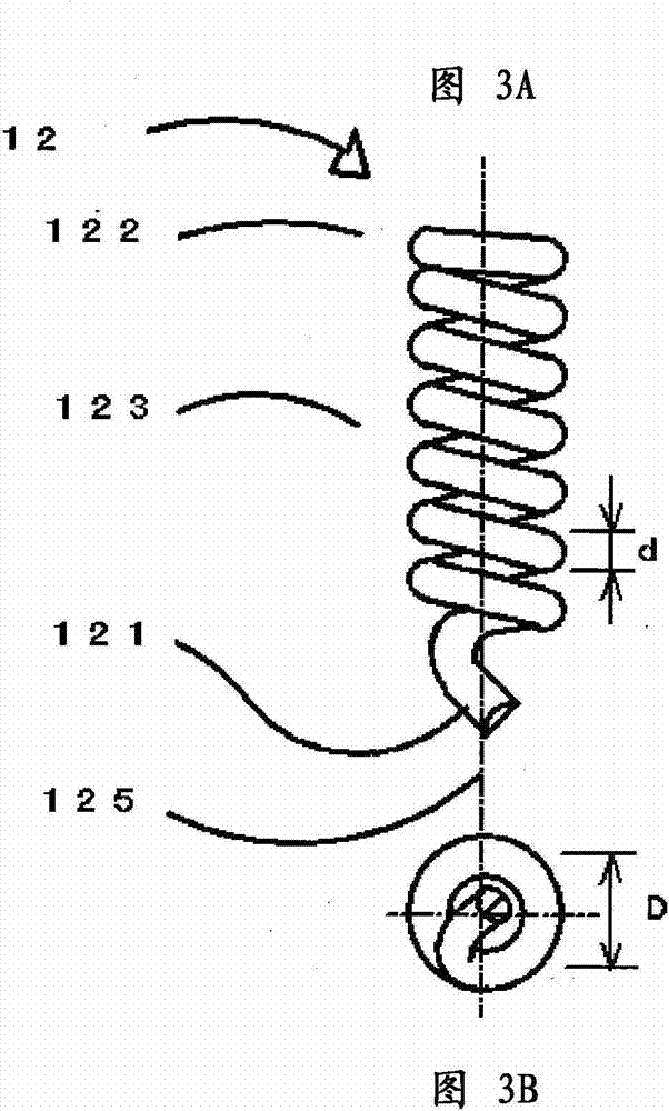
[0089] When inspecting a through-hole printed circuit board, there may be a through hole area (through hole land) as an inspection terminal. There is a hole in the through-hole area, into which the protruding part 112 of the contact 10 enters to cause poor contact, thus requiring a contact pin 11 whose diameter of the protruding part 112 is larger than that of the hole. The load, wire diameter, and outer diameter of the coil spring 12 also increase. When mixed with thin-diameter contacts 10 used for inspection terminals in non-porous surface mount areas, it is also possible to increase the range of electrodes 41 with the same diameter, thereby increasing the ease of design and manufacture. When the physical strength of the coil spring 12 with a large load is not enough, it is preferable to use Figure 4C cut in the circumferential direction.
PUM
 Abstract
Description
Claims
Application Information