Wafer temperature detection method

A detection method and wafer technology, applied in the direction of semiconductor/solid-state device testing/measurement, etc., can solve the problems of low temperature detection efficiency and inaccurate detection of wafer temperature, achieve good linear characteristics, improve accuracy, and increase application range effect

Active Publication Date: 2013-04-17
SHANGHAI HUAHONG GRACE SEMICON MFG CORP
View PDF7 Cites 13 Cited by
  • Summary
  • Abstract
  • Description
  • Claims
  • Application Information

AI Technical Summary

Problems solved by technology

[0006] In the existing MOS transistor manufacturing or analysis testing, the wafer is usually placed on the stage of the processing equipment, and then the wafer is heated by contact or non-contact through the heating device on the stage. The temperature sensor on the stage detects the heating temperature, and the temperature detected by the temperature sensor on the stage is the temperature of the wafer, but this method cannot accurately detect the temperature of the wafer itself, and the efficiency of temperature detection is low

Method used


Image

  • Wafer temperature detection method
  • Wafer temperature detection method
  • Wafer temperature detection method

Examples


Embodiment Construction

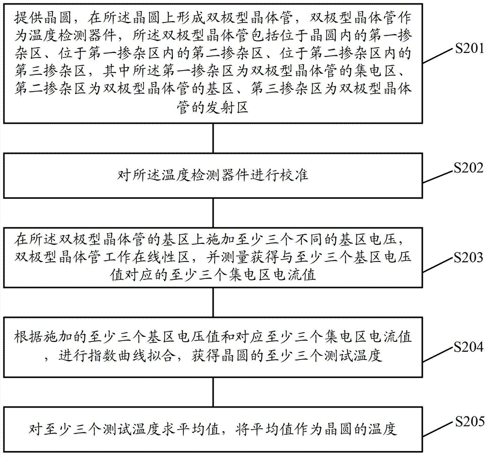
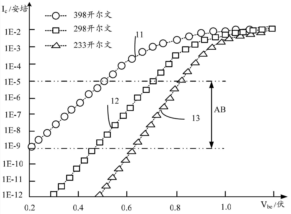
[0030] In the existing heating device for heating the wafer, the heat is transferred to the wafer through heat conduction or radiation, and when the temperature is detected, the stage or the processing chamber is generally controlled in a contact or non-contact manner. Therefore, the detected temperature is not necessarily the actual temperature inside the wafer. There is a difference between the detected temperature and the actual temperature, which is not conducive to the improvement of the performance of semiconductor devices and the establishment of related models. It takes a long time for temperature stabilization (generally more than 30 minutes) during heating to make the actual temperature in the wafer close to the set temperature of heating, which makes the whole measurement process take a long time and the efficiency is low.

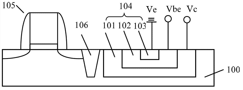
[0031] In order to solve the above problems, the inventor proposes a method for detecting the temperature of the wafer, forming a bipolar transi...


PUM


Abstract

The invention discloses a wafer temperature detection method. The wafer temperature detection method comprises the following steps of: providing a wafer; forming a bipolar transistor on the wafer and taking the bipolar transistor as a temperature detection device; calibrating the temperature detection device; applying at least three different base region voltages to the base region of the bipolar transistor in turn, making the bipolar transistor work in a linear region, and measuring to obtain at least three collecting region current values corresponding to the three base region voltage values; and performing exponential curve fitting according to the three applied base region voltage values and the at least three corresponding collecting region current values to obtain at least three test temperatures of the wafer; and solving the mean value of the at least three test temperatures, and taking the mean value as the temperature of the wafer. The accuracy and the efficiency of the temperature detection are improved.

Description

technical field [0001] The invention relates to the field of semiconductor manufacturing, in particular to a method for detecting the temperature of a wafer. Background technique [0002] In the existing integrated circuit manufacturing, with the continuous advancement of semiconductor integrated circuit technology and the continuous reduction of feature size, the number of devices on a single wafer has continued to increase, the function of the circuit has been improved, the circuit has become increasingly complex, and the process The links in manufacturing are required to be more and more refined, and the reliability of devices is becoming more and more important. [0003] Metal-oxide-semiconductor (MOS) transistors are the most basic devices in semiconductor manufacturing. They are widely used in various integrated circuits. According to the main carrier and the type of doping during manufacturing, they are divided into NMOS and PMOS transistors. [0004] However, the ex...

Claims


Application Information

Patent Timeline
Patent Type & Authority Applications(China)
IPC IPC(8): H01L21/66
Inventor 范象泉张昊
Owner SHANGHAI HUAHONG GRACE SEMICON MFG CORP
Why Eureka
Try Eureka