Spacer for semiconductor structure contact
A technology of spacers and semiconductors, used in semiconductor devices, semiconductor/solid-state device manufacturing, semiconductor/solid-state device components, etc.
- Summary
- Abstract
- Description
- Claims
- Application Information
AI Technical Summary
Problems solved by technology
Method used
Image

Examples
Embodiment Construction
[0028] The making and using of embodiments of the invention are discussed in detail below. It should be appreciated, however, that the present invention provides many applicable inventive concepts that can be embodied in a wide variety of specific contexts. The specific embodiments discussed are merely illustrative of specific ways to make and use the disclosed subject matter, and do not limit the scope of the invention.
[0029] Embodiments will be described in context, namely, semiconductor devices and structures having epitaxially grown regions and contacts of the epitaxial regions. Other embodiments may apply to structures having regions of similar geometry to which contacts are formed, but which may not include epitaxial growth.
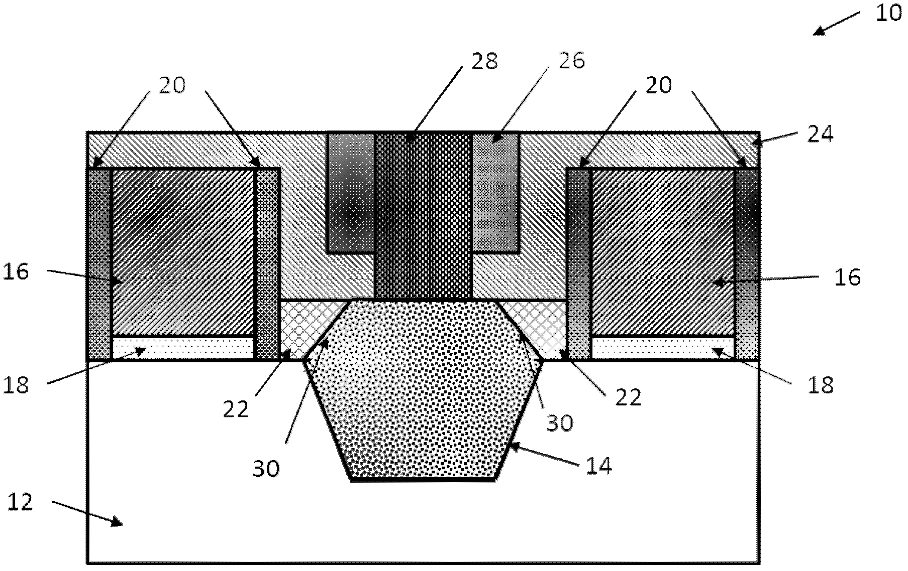
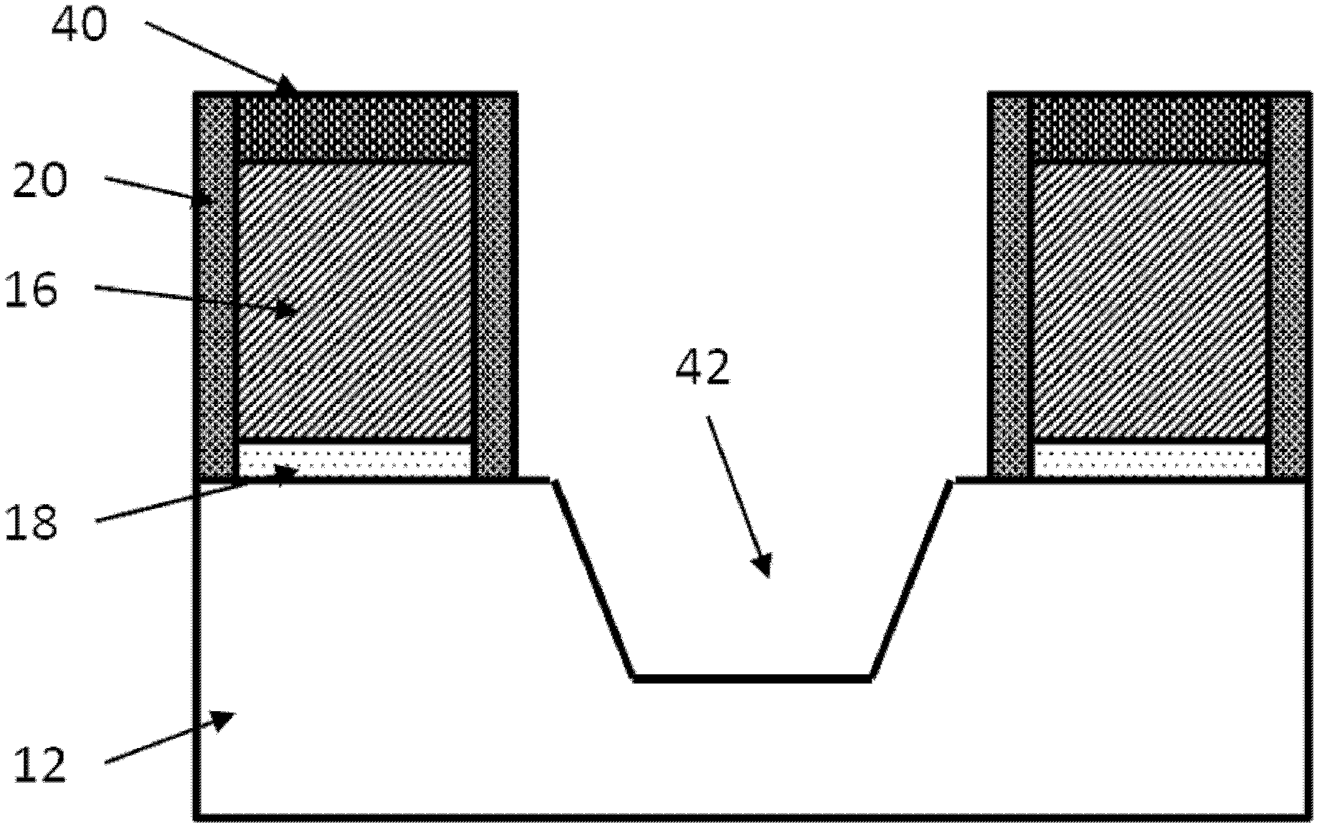
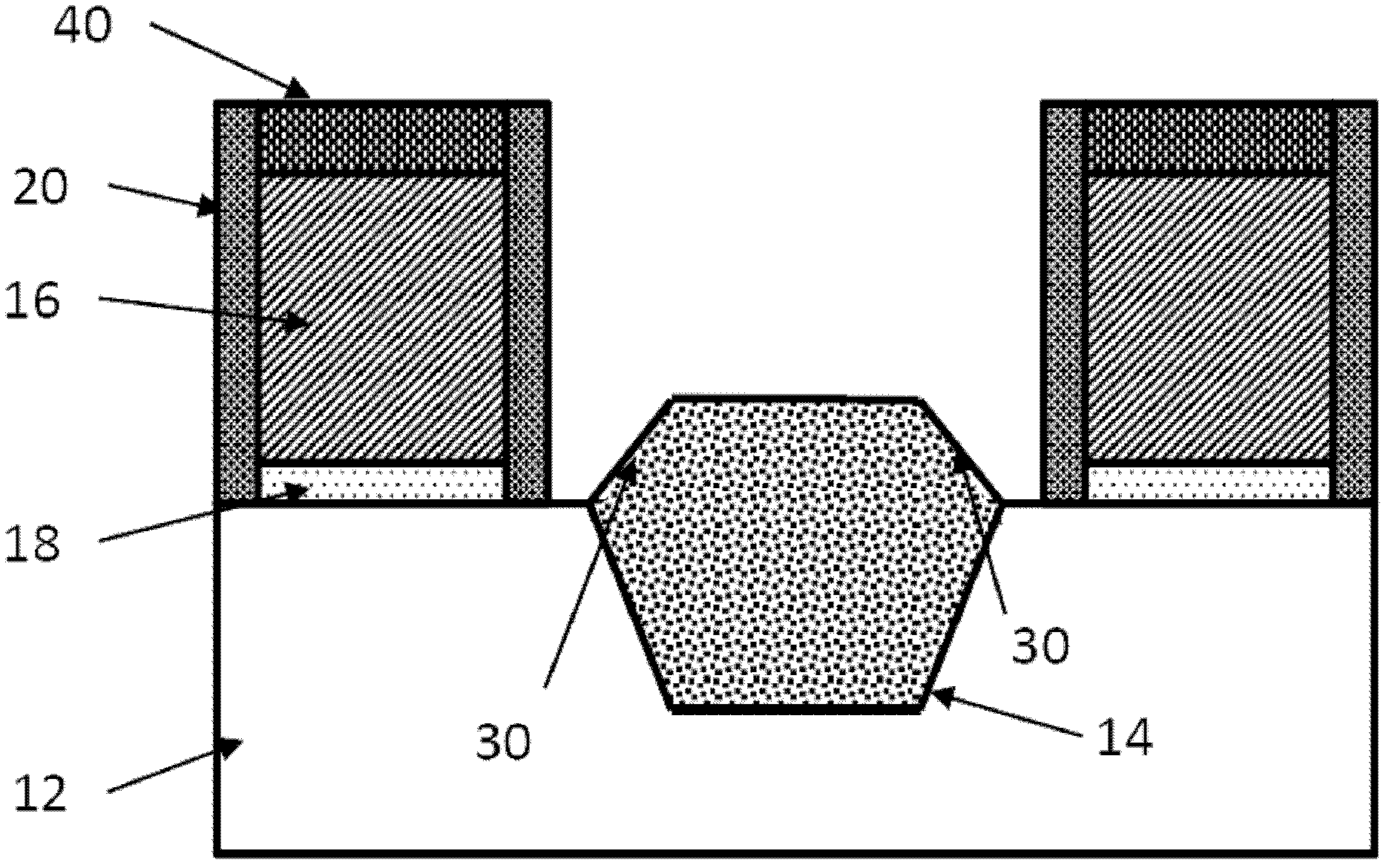
[0030] figure 1 A semiconductor structure 10 according to an embodiment is shown. The structure includes: a substrate 12, an epitaxial region 14, a gate 16 over a corresponding gate dielectric layer 18, a gate spacer 20 along the sidewalls of...
PUM
 Abstract
Description
Claims
Application Information
 - R&D
- Intellectual Property
- Life Sciences
- Materials
- Tech Scout
- Unparalleled Data Quality
- Higher Quality Content
- 60% Fewer Hallucinations
Browse by: Latest US Patents, China's latest patents, Technical Efficacy Thesaurus, Application Domain, Technology Topic, Popular Technical Reports.
© 2025 PatSnap. All rights reserved.Legal|Privacy policy|Modern Slavery Act Transparency Statement|Sitemap|About US| Contact US: help@patsnap.com