
Pressing method for sandwich aluminum-base printed circuit board

A technology for printed circuit boards and aluminum substrates, used in printed circuits, printed circuit manufacturing, electrical components, etc., can solve the problems of resin voids in the holes, bowing of the board, and inability to fill the through holes of aluminum substrates, and achieves increased bonding. force effect

Inactive Publication Date: 2013-04-17
SHENZHEN SUNTAK MULTILAYER PCB +1
View PDF3 Cites 20 Cited by
  • Summary
  • Abstract
  • Description
  • Claims
  • Application Information

AI Technical Summary

Problems solved by technology

[0006] For this reason, the object of the present invention is to provide a kind of sandwich aluminum-based printed circuit board lamination method, to solve the current multi-layer sandwich aluminum-based printed circuit board in lamination production, due to the poor combination of prepreg and aluminum-based surface, and It is prone to problems of delamination, bowing and twisting of the board
[0007] In addition, the purpose of the present invention is also to provide a method for laminating aluminum-based printed circuit boards, so as to solve the problem that the current multi-layer sandwich aluminum-based printed circuit boards cannot be through-holed due to the limited thickness of the prepreg. Filled, prone to the problem of resin voids in the hole

Method used

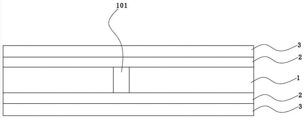
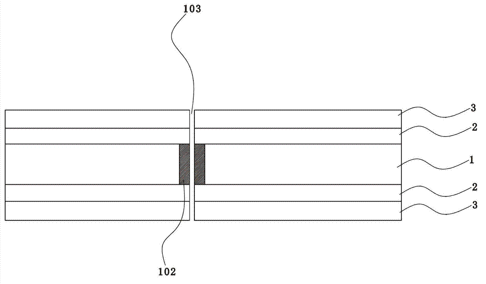

Image

  • Pressing method for sandwich aluminum-base printed circuit board
  • Pressing method for sandwich aluminum-base printed circuit board
  • Pressing method for sandwich aluminum-base printed circuit board

Examples


Embodiment Construction

[0028] In order to illustrate the idea and purpose of the present invention, the present invention will be further described below in conjunction with the accompanying drawings and specific embodiments.

[0029] The core idea of ​​the present invention is: fill resin in the through hole on the aluminum substrate, and carry out wire drawing treatment on the upper and lower surfaces of the aluminum substrate, so that the surface of the aluminum substrate forms a pattern of lines, and then paste prepreg on the upper and lower surfaces of the aluminum substrate, and on the prepreg Cover the copper foil layer, then laminate the board to make a sandwich aluminum-based printed circuit board, and finally drill a hole in the sandwich aluminum-based printed circuit board so that the hole in the hole penetrates the entire board, and It is located in the aluminum substrate filling resin, so that the connection between the upper and lower copper foil layers is formed.

[0030] See figure ...


PUM


Abstract

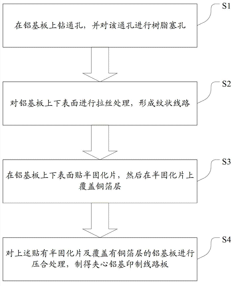
The invention discloses a pressing method for a sandwich aluminum-base printed circuit board. The pressing method comprises the following steps of: S1, drilling a through hole in an aluminum substrate and filling the through hole with resin; S2, performing wire drawing treatment on upper and lower surfaces of the aluminum substrate to form wavelike circuits; S3, attaching semi-cured sheets to the upper and lower surfaces of the aluminum substrate and then covering the semi-cured sheets with a copper foil layer; and S4, pressing the aluminum substrate to which the semi-cured sheets are attached and which is covered by the copper foil layers to prepare the sandwich aluminum-base printed circuit board. According to the pressing method, the wire drawing treatment is performed on the upper and lower surfaces of the aluminum substrate to enhance the binding force of the semi-cured sheets and the upper and lower surfaces of the aluminum substrate; temperature and pressure in a pressing process are controlled, so that the surfaces of the entire aluminum substrate can be filled better by the semi-cured sheets; and the resin is filled in the through hole in the aluminum substrate, and an in-hole hole is drilled in the sandwich aluminum-base printed circuit board after pressing, so that connection of lines between the upper and lower copper foils is realized, and the problem of short circuiting due to conduction of an outer layer circuit and the aluminum substrate caused by resin cavitation in the through hole of the aluminum substrate is solved.

Description

Technical field: [0001] The invention belongs to the technical field of printed circuit board production, and specifically relates to a pressing method for sandwich aluminum-based printed circuit boards. Background technique: [0002] With the rapid progress and development of electronic technology, it has become an inevitable trend for electronic products to develop in the direction of "light, short, thin, small", personalized, high reliability and multi-functional. At present, most double-sided boards and multi-layer boards are FR4 and CEM3 are used as printed board substrates. Due to the high integration and high power of electronic components on the circuit board, the heat generation also increases correspondingly. However, the existing FR4 and CEM3 printed board substrates are all hot Poor conductors prevent the generated heat from dissipating through the circuit board in time, which will easily lead to high temperature failure of electronic components on the circuit bo...

Claims


Application Information

Patent Timeline
Patent Type & Authority Applications(China)
IPC IPC(8): H05K3/00
Inventor 张军杰姜雪飞李学明刘东宋建远
Owner SHENZHEN SUNTAK MULTILAYER PCB
Learn More