Bireflection light emitting diode

A technology of light-emitting diodes and reflective surfaces, applied in electrical components, circuits, semiconductor devices, etc., can solve problems such as unfavorable light output efficiency, and achieve the effect of increasing light output efficiency

Inactive Publication Date: 2013-05-01
AQUALITE CO LTD
View PDF4 Cites 10 Cited by
  • Summary
  • Abstract
  • Description
  • Claims
  • Application Information

AI Technical Summary

Problems solved by technology

[0002] The metal electrodes on the surface of the LED chip structure can make the current spread better, but the photons will be absorbed or reflected by the contacted metal when they are on the path of light emission, and the reflected photons may be absorbed, which is not conducive to improving the light output efficiency.

Method used


Image

  • Bireflection light emitting diode
  • Bireflection light emitting diode
  • Bireflection light emitting diode

Examples


Embodiment 1

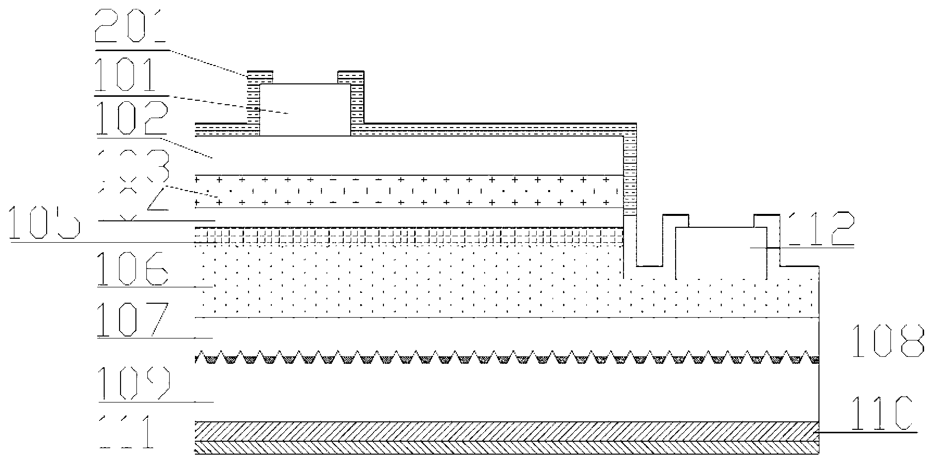
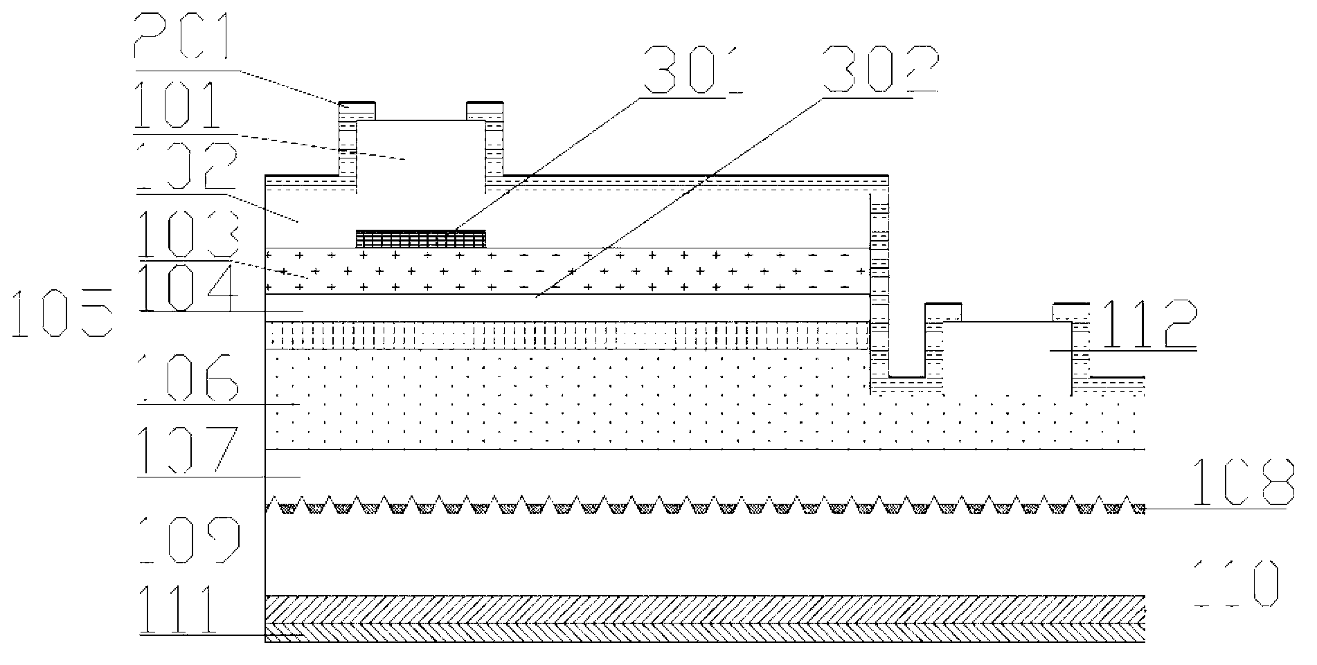
[0026] Embodiment 1: as figure 2 As shown, the current spreading layer 102 is used for double reflection.

[0027] The first light reflecting surface 301 is located between the lower surface of the P electrode 101 and the upper surface of the current spreading layer 102 , and the second light reflecting surface 302 is located between the lower surface of the current spreading layer 102 and the upper surface of the P-type layer 103 .

[0028] A preferred embodiment of the first light reflection surface 301 is a newly added Bragg reflection layer between the lower surface of the P electrode 101 and the upper surface of the current spreading layer 102, that is, a multilayer structure in which SiO2 and TiO2 are alternately combined, such that Reflection works best. Alternatively, the first light reflection surface 301 can also be an omnidirectional reflection layer, or a newly added layer of Ag or Al, which has better reflection effect; or, the first reflection surface 301 itsel...

Embodiment 2

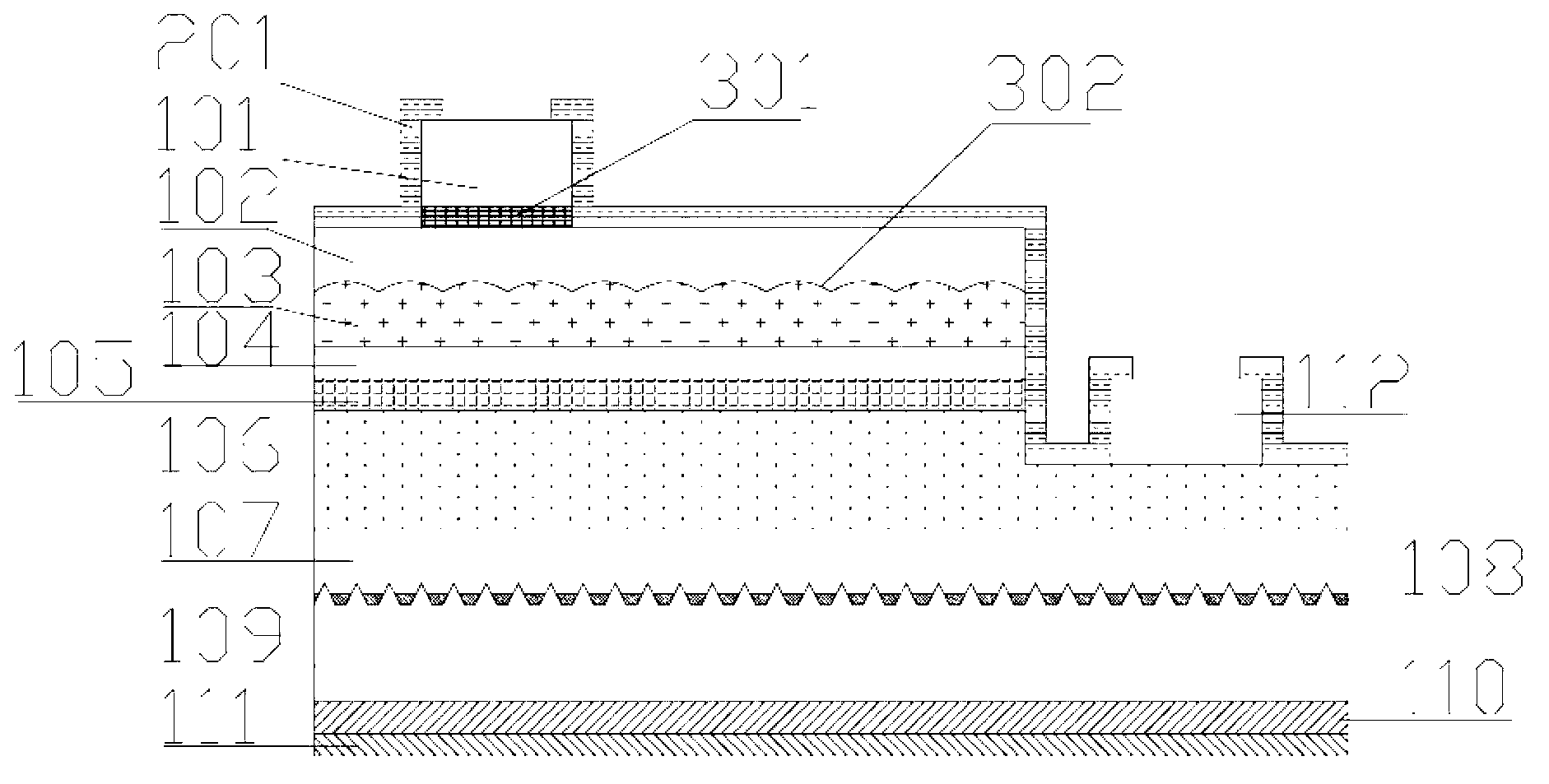
[0031] Embodiment 2: as image 3 As shown, the P-type layer 103 is used for double reflection.

[0032] The first light reflecting surface 301 is located between the lower surface of the current spreading layer 102 and the upper surface of the P-type layer 103 , and the second light reflecting surface 302 is located between the lower surface of the P-type layer 103 and the upper surface of the active layer 105 .

[0033] The preferred embodiment of the first light reflecting surface 301 is also a newly added Bragg reflective layer; if this is the case, it is further preferred to describe a solution similar to that in Example 1, that is, the area of ​​the newly added Bragg reflective layer is greater than or equal to the P electrode The area of ​​the lower surface of the P electrode 101 is smaller than the area of ​​the lower surface of the current spreading layer 102, and the projection of the lower surface of the P electrode 101 on the Bragg reflection layer falls completely ...


PUM


Abstract

The invention relates to a bireflection light emitting diode, which comprises a P electrode, a current expansion layer, a P type layer and an active layer, wherein the P electrode, the current expansion layer, the P type layer and the active layer are successively arranged from top to bottom, and a first ray reflection surface and a second ray reflection surface are respectively arranged on different heights between the lower surface of the P electrode and the upper surface of the active layer. According to the bireflection light emitting diode disclosed by the invention, light is continuously reflected and scattered between the two reflection surfaces so as to increase the luminous efficiency of the light emitting diode.

Description

technical field [0001] The invention relates to the technical field of light emitting diodes, in particular to a light emitting diode with a reflective structure. Background technique [0002] The metal electrodes on the surface of the LED chip structure can make the current spread better, but the photons will be absorbed or reflected by the contacted metal when they are on the path of light emission, and the reflected photons may be absorbed, which is not conducive to improving the light output efficiency. . Contents of the invention [0003] The technical problem to be solved by the present invention is to provide a light-emitting diode that increases the light extraction rate by arranging double reflective layers. [0004] The technical solution of the present invention to solve the above-mentioned technical problems is as follows: a light-emitting diode, including a P electrode, a current spreading layer, a P-type layer and an active layer arranged in sequence from to...

Claims


Application Information

Patent Timeline
Patent Type & Authority Applications(China)
IPC IPC(8): H01L33/10H01L33/14
Inventor 王汉华项艺杨新民靳彩霞董志江
Owner AQUALITE CO LTD
Why Eureka
Try Eureka