Optimization method of capturing power consumption in scan test

An optimization method and scanning test technology, applied in electronic circuit testing, special data processing applications, instruments, etc., can solve the problems of increasing test design complexity and prolonging test time, and achieve the effect of reducing capture power consumption and easy implementation.

Inactive Publication Date: 2013-05-08
JIANGSU SEUIC TECH CO LTD
View PDF6 Cites 24 Cited by
  • Summary
  • Abstract
  • Description
  • Claims
  • Application Information

AI Technical Summary

Problems solved by technology

Similar to reducing the test clock frequency, this method also increases the test time
Moreover, this block test method needs to modify the circui

Method used


Image

  • Optimization method of capturing power consumption in scan test
  • Optimization method of capturing power consumption in scan test
  • Optimization method of capturing power consumption in scan test

Examples


Embodiment Construction

[0021] The present invention will be described in further detail below in conjunction with the accompanying drawings.

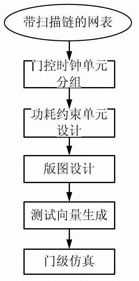
[0022] The invention analyzes the test power consumption of each part in detail, focuses on reducing the capture test power consumption, and finally provides a low power consumption test scheme based on the power consumption optimization of the gating clock. On the basis of the basic test flow, the present invention adds two steps of gate control clock unit grouping and power consumption constrained unit design, the technical scheme is as follows figure 1 As shown, the overall process is as follows:

[0023] (1) Generate a netlist with a scan chain. Described as follows:

[0024] ① Carry out testability analysis on the RTL code of the chip, and modify the RTL code of the chip.

[0025] ② Use the process library provided by the process manufacturer to map the modified RTL code into a gate-level netlist, and at the same time, according to the design constrai...


PUM


Abstract

The invention discloses an optimization method of capturing power consumption in a scan test. The optimization method of capturing power consumption in the scan test comprises the following steps: generating a netlist with a scan chain; grouping gating control clock units; designing a power constrain unit; combining with the generated netlist with the scan chain, conducting chip layout design which comprises a floorpan, a layout, a clock tree sythesis and wiring; reading a gate-level netlist with a scan structure, a process library, a timing sequence constrain file and a test protocol into an automatic test vector generating tool after the chip layout design is completed, conducting testability design rule checking, and generating a test vector; and conducting gate-level simulation to the test vector generated. By means of the optimization method of capturing the power consumption in the scan test, the capturing power consumption in a test process can be reduced significantly, the reduction of coverage or the sharp increase of the quantity of test vectors is not generated, changing of a test design process is needless, and realization is easy.

Description

technical field [0001] The invention belongs to the technical field of chip low power consumption test design, and in particular relates to an optimization method aiming at capturing power consumption in scanning test. Background technique [0002] With the continuous shrinking of the physical size of integrated circuits and the continuous reduction of voltage thresholds, power consumption, performance, and area have become the most important design indicators for system chip design. In the last decade, low-power design based on algorithms, architectures, and circuits has attracted great attention, and chip designers are increasingly adopting low-power designs to meet increasingly difficult power consumption challenges. While low-power design methodologies can address power consumption issues that arise in the design of complex digital systems, they are not very effective for power consumption in test modes. Studies have shown that the power consumption of LSI in test mode ...

Claims


Application Information

Patent Timeline
IPC IPC(8): G01R31/28G06F17/50
Inventor 蔡志匡陈慧黄丹丹李哲文邵金梓
Owner JIANGSU SEUIC TECH CO LTD
Why Eureka
Try Eureka