Method for extracting base parasitic resistance from HBT component

A technology of parasitic resistance and base area, applied in the direction of instruments, electrical digital data processing, special data processing applications, etc., can solve the problems of large errors and inability to adapt to the model, and achieve the effect of improving accuracy

Active Publication Date: 2013-05-08
SHANGHAI HUAHONG GRACE SEMICON MFG CORP
View PDF4 Cites 6 Cited by
  • Summary
  • Abstract
  • Description
  • Claims
  • Application Information

AI Technical Summary

Problems solved by technology

However, since the square value of the base parasitic resistance in HBT is very small, it is greatly affected by the doping concentration, and the size of the ordinary straight strip resistor is very different from the size of the base silicon germanium polysilicon in the actual HBT device. The error introduced by the outside is also very large, so the resistance value extracted by the straight resistor cannot meet the needs of the model

Method used


Image

  • Method for extracting base parasitic resistance from HBT component
  • Method for extracting base parasitic resistance from HBT component
  • Method for extracting base parasitic resistance from HBT component

Examples


Embodiment Construction

[0021] The method for extracting the base parasitic resistance in the HBT device of the present invention comprises the following steps:

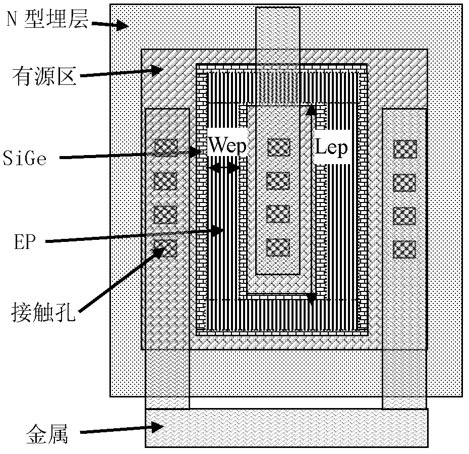
[0022] first step, such as figure 2 As shown, the cross-section is rectangular ring-shaped EP (emitter polysilicon), and the link resistance (connection resistance) of SiGe Poly is formed through the shielding of rectangular ring-shaped EP;

[0023] The strip width of the rectangular ring EP is Wep, and the length is Lep;

[0024] The strip width Wep and the length Lep of the rectangular annular EP take different values ​​to obtain a set of linear change values, and the precise resistance value is deduced by fitting on the device model.

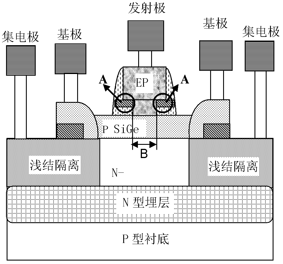
[0025] Such as image 3 As shown, A is the parasitic Link resistance of the base of the HBT, which is directly below the EP. Since it will be shielded by the rectangular ring EP during the alloying (silicide) process, it cannot be alloyed;

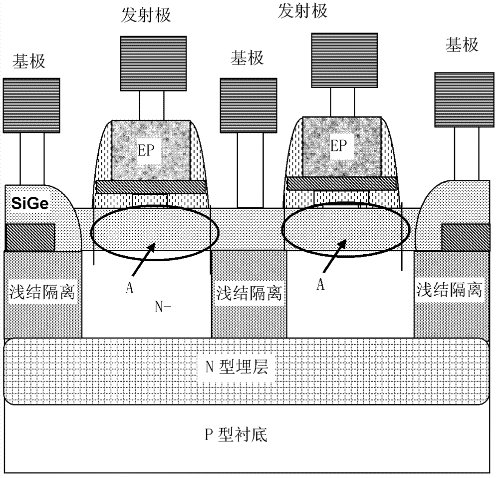
[0026] The second step, such as Figure 4 As shown, a rectan...


PUM


Abstract

The invention discloses a method for extracting base parasitic resistance from HBT (Heterojunction Bipolar Transistor)components. The method includes steps: 1, utilizing an emitter polycrystalline silicon with rectangular and circular cross section, through the shielding of the rectangular and circular emitter polycrystalline silicon, to form a connecting resistance of a germanium-silicon polycrystalline silicon; taking different values of strip width and length of the rectangular and circular emitter polycrystalline silicon to obtain a group of linear change values, and calculating accurate resistance value by fitting on a component model; 2, opening a rectangular and circular emitter region window at the rectangular and circular emitter polycrystalline silicon to form a base window resistance of the germanium-silicon polycrystalline silicon, taking different values of strip width and length of the rectangular and circular emitter region window to obtain a group of linear change values, and calculating accurate resistance value by fitting on a component model. The invention can accurately extract SiGe Poly parasitic resistances and effectively improve accuracy of the component model, therefore a better instruction for system-level simulation is provided.

Description

technical field [0001] The invention relates to a monitoring method of a heterojunction bipolar transistor, in particular to a method for extracting parasitic resistance of a base region in an HBT device. Background technique [0002] HBT (heterojunction bipolar transistor) device structure such as figure 1 shown. In the HBT device, the parasitic resistance of silicon germanium polysilicon (SiGe Poly) in the base region will become an important factor affecting the frequency characteristics of the HBT. [0003] Most of the existing structures used to extract the parasitic resistance of the base region in the HBT device are ordinary straight strip resistors. Specifically, a straight bar-shaped silicon-germanium-silicon polysilicon in the base area is used, and a corresponding resistance value is extracted through a set of structures whose length and width vary. However, since the square value of the base parasitic resistance in HBT is very small, it is greatly affected by ...

Claims


Application Information

Patent Timeline
Patent Type & Authority Applications(China)
IPC IPC(8): G06F17/50
Inventor 苗彬彬朱丽霞金锋
Owner SHANGHAI HUAHONG GRACE SEMICON MFG CORP
Why Eureka
Try Eureka