An optimal design method for electrical properties of optoelectronic integrated packaging structures

A technology of electrical performance optimization and packaging structure, applied in computing, electrical digital data processing, instruments, etc., can solve the problems of heavy workload, low efficiency, poor precision, etc., and achieve the effect of improving electrical performance, convenient use, and optimized design

Inactive Publication Date: 2016-04-06
EAST CHINA NORMAL UNIV
View PDF0 Cites 0 Cited by
  • Summary
  • Abstract
  • Description
  • Claims
  • Application Information

AI Technical Summary

Problems solved by technology

The problems existing in the prior art are: using formula formulas to carry out the optimization design of manual calculation, the workload is heavy, the precision is poor, and the efficiency is low

Method used


Image

  • An optimal design method for electrical properties of optoelectronic integrated packaging structures

Examples


Embodiment Construction

[0019] (1) Establish a three-dimensional geometric model of the package structure

[0020] Open the AnsoftHFSS interface (the version used is HFSS-9), use the HFSS software library to establish a three-dimensional geometric model of the adjacent pads of the package, and mark the pad diameter as 100um, the pad spacing as 40um, the substrate thickness as 300um, and the gap width as Structural parameters of 12um and signal line width of 100um.

[0021] (2) Establish an RC equivalent circuit

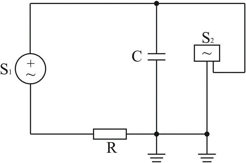
[0022] See attached figure 1 , input the above three-dimensional geometric model parameters into the HFSS simulation software, and then use the finite element program of HFSS, combined with the geometric structure parameters of the package to capture the resistance R of the equivalent circuit is 46.52Ω, the capacitance C is 0.0125pF, the resistance R and capacitance C and AC signal source S 1 Form a series circuit and connect the oscilloscope S 2 Parallel to both ends of the capacitor C,...


PUM


Abstract

The invention discloses an electric performance optimization design method of a photoelectricity integration packaging structure. The performance optimization design method of the photoelectricity integration packaging structure is characterized in that when packaging electrical performance design of a photoelectricity component and a reading integrated circuit (IC) module is conducted, high frequency structure simulator (HFSS) software is applied to electrical performance simulation of a packaging structure, by co-simulation with electronic webbench (EWB) or POWERPCB software, input port signal pad crosstalk and interference are simulated, and thus electrical features of the package structure is optimized. Compared with the prior art, the performance optimization design method of the photoelectricity integration packaging structure is high in accuracy, and convenient to use, and avoids a manpower operation step, can well solve the problem of crosstalk of a signal port and a channel by design simulation, reduces stray inductance, a capacitance, resistance and produced noise of the packaging structure, improves electrical performance of the package structure, effectively avoids failure, and reduces cost.

Description

technical field [0001] The invention relates to the technical field of electronics and circuit design, in particular to an electrical performance optimization design method of an optoelectronic integrated packaging structure. Background technique [0002] In recent years, as the feature size of integrated circuits has entered the nanometer scale, the electrical properties of the packaging structure have an increasing impact on the performance of optoelectronic integrated modules and RF integrated circuits. Packaging design greatly affects signal integrity and may make circuits Failed at runtime. The electrical properties of the package structure mainly include pad and lead resistance, insulation resistance between leads, pad and lead capacitance and load capacitance, pad and lead inductance, etc., which must be detected and controlled to accurately and quickly estimate the inductance of the package structure. crosstalk effects. Optimizing the design by means of simulation ...

Claims


Application Information

Patent Timeline
Patent Type & Authority Patents(China)
IPC IPC(8): G06F17/50
Inventor 葛羽屏郭方敏郑正奇
Owner EAST CHINA NORMAL UNIV
Why Eureka
Try Eureka