Semiconductor device having lid structure and method of making same

A semiconductor and device technology, applied in the field of semiconductor packaging, can solve problems such as impact, unfavorable die performance, and reduced heat dissipation capacity

Inactive Publication Date: 2013-05-15
TAIWAN SEMICON MFG CO LTD
View PDF3 Cites 5 Cited by
  • Summary
  • Abstract
  • Description
  • Claims
  • Application Information

AI Technical Summary

Problems solved by technology

However, along with heat generation, the die may also work in a high humidity operating environment
Higher levels of moisture can enter the semiconductor package and adversely affec...

Method used


Image

  • Semiconductor device having lid structure and method of making same
  • Semiconductor device having lid structure and method of making same
  • Semiconductor device having lid structure and method of making same

Examples


Embodiment Construction

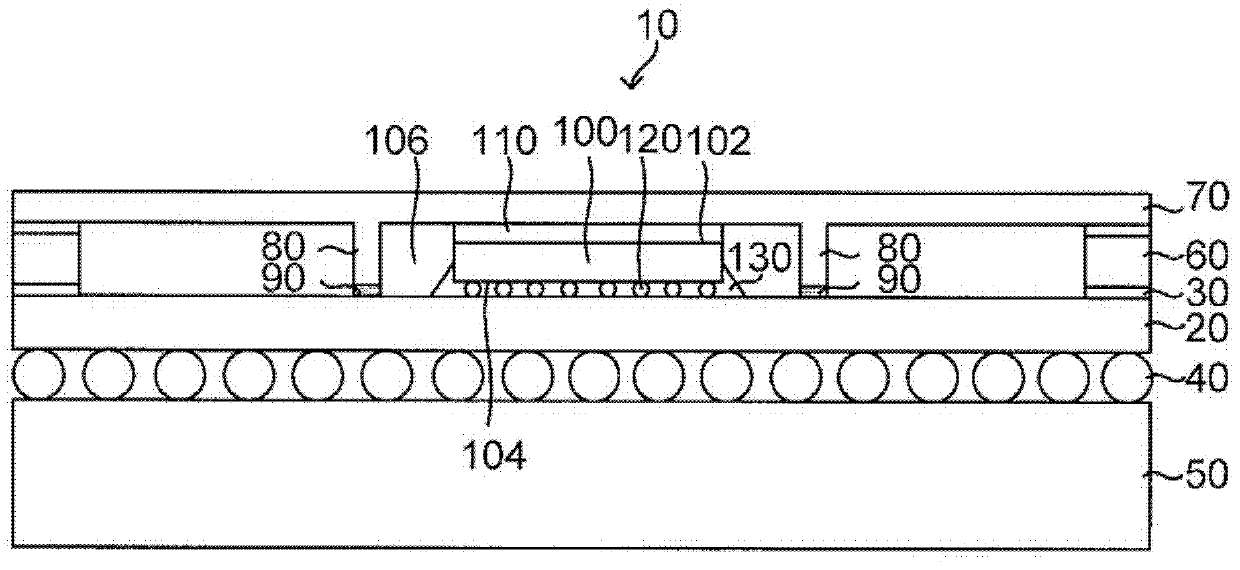
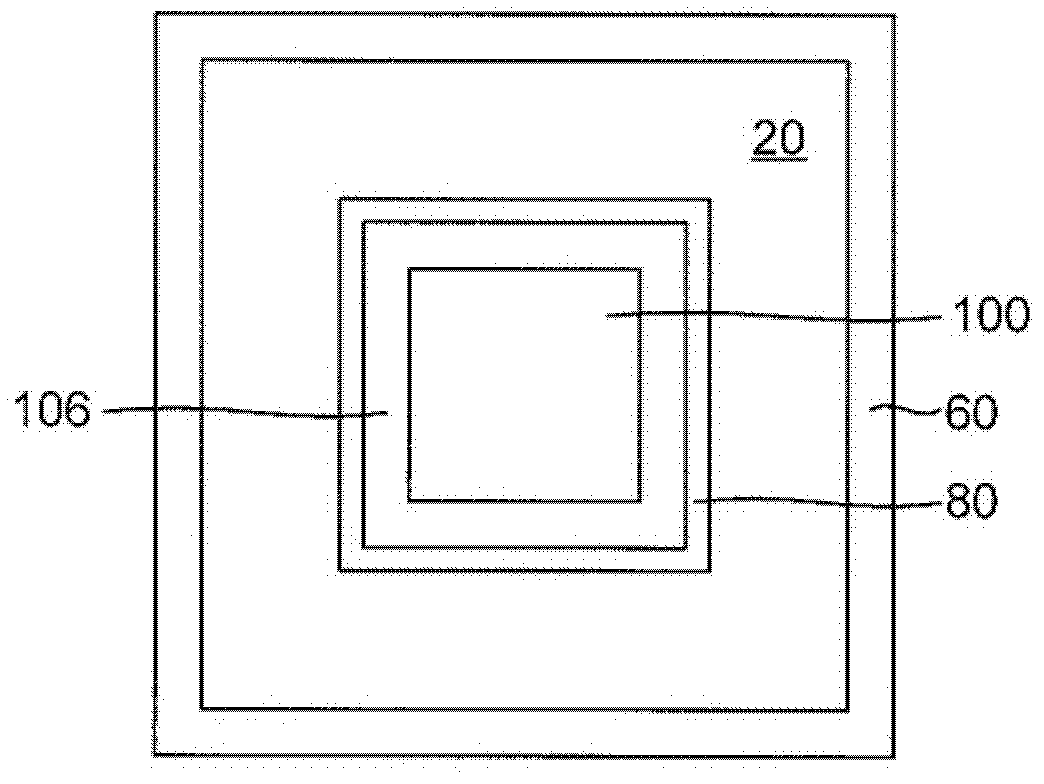
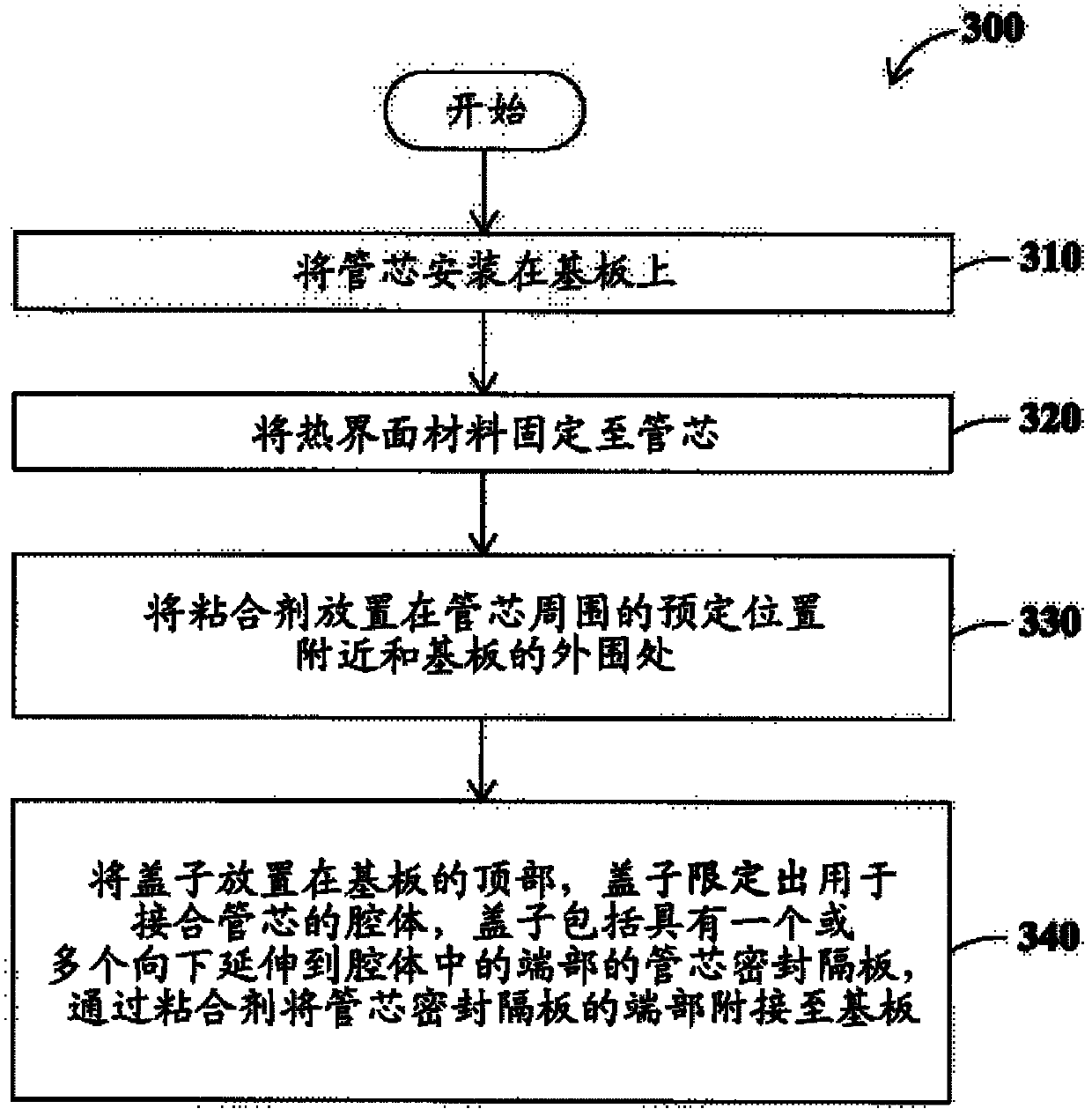
[0029] In the following description, numerous specific details are set forth in order to provide a thorough understanding of embodiments of the invention. However, one of ordinary skill in the art will recognize that embodiments of the invention may be practiced without these specific details. In some instances, well-known structures and processes have not been described in detail so as not to unnecessarily obscure the embodiments of the present invention.

[0030] Reference throughout this specification to "one embodiment" or "an embodiment" means that at least one embodiment of the present invention includes a particular component, structure or feature described in connection with the embodiment. Thus, appearances of the phrases "in one implementation" or "in an embodiment" in various places in this specification are not necessarily referring to the same embodiment. Furthermore, particular components, structures or features may be combined in any suitable manner in one or m...


PUM


Abstract

A semiconductor device includes a substrate, a first die attached to the substrate, and a lid coupled to the substrate. The lid defines a cavity for engaging the first die, and the lid has a die enclosure barrier having ends extending downwardly into the cavity. The ends of the die enclosure barrier are attached to the substrate and a thermal interface material is disposed between the first die and the lid, thermally connecting the first die to the lid.

Description

technical field [0001] The present invention relates generally to semiconductor devices, and more particularly, to semiconductor packages for semiconductor devices. Background technique [0002] Today, semiconductor devices typically include: a die, a substrate, a heat sink, a thermal interface material (TIM) for connecting the die to the heat sink, one or more metallization layers, input / output (I / O) pins or ball and optional heat sink. The die has source circuit devices and is typically mounted on a substrate or within a cavity in the substrate. Since the active side of the die faces down, such semiconductor devices are often referred to as "flip-chip" packages. [0003] In modern semiconductor packages, the relentless pursuit of higher performance and smaller size has resulted in higher operating frequencies and ever-increasing packing densities (more transistors per unit area). During operation, the circuits on such a die consume a large amount of electrical energy, w...

Claims


Application Information

Patent Timeline
IPC IPC(8): H01L23/04H01L23/36H01L21/52
CPCH01L23/04H01L2924/15311H01L2224/73204H01L21/50H01L2224/32225H01L23/42H01L2224/73253H01L23/3675H01L23/36H01L2924/0002H01L23/10H01L21/52H01L2224/16225H01L2924/00
Inventor 林文益林柏尧
Owner TAIWAN SEMICON MFG CO LTD
Why Eureka
Try Eureka