Capacitive control screen with three-dimensional via hole and manufacturing method thereof

A manufacturing method and technology of via holes, which are applied in the direction of electrical digital data processing, input/output process of data processing, instruments, etc., can solve the problem that the conductive interface is difficult to control, the insulating layer is difficult, and the position of the via hole is brittle. and other problems, to achieve the effect of improving the overall process quality, simplifying the manufacturing process, and increasing reliability

Active Publication Date: 2013-06-12
宏科有限公司
View PDF5 Cites 10 Cited by
  • Summary
  • Abstract
  • Description
  • Claims
  • Application Information

AI Technical Summary

Problems solved by technology

[0003] The commonly used method of making via holes in the industry is to directly punch holes on double-sided circuit boards, and then inject conductive medium to form via holes. This method is easy to damage the circuit board, especially when the circuit board needs to be bent, the conduction The hole position is prone to brittle fracture
Especially in the process of capacitive control panels with high requirements for thin thickness and precision, it is extremely difficult to use insulating layers to make three-dimensional via holes. At the same time, it is difficult to control the conductive interface, so three-dimensional via holes have not been applied In the process of capacitive control panel

Method used


Image

  • Capacitive control screen with three-dimensional via hole and manufacturing method thereof
  • Capacitive control screen with three-dimensional via hole and manufacturing method thereof

Examples


Embodiment Construction

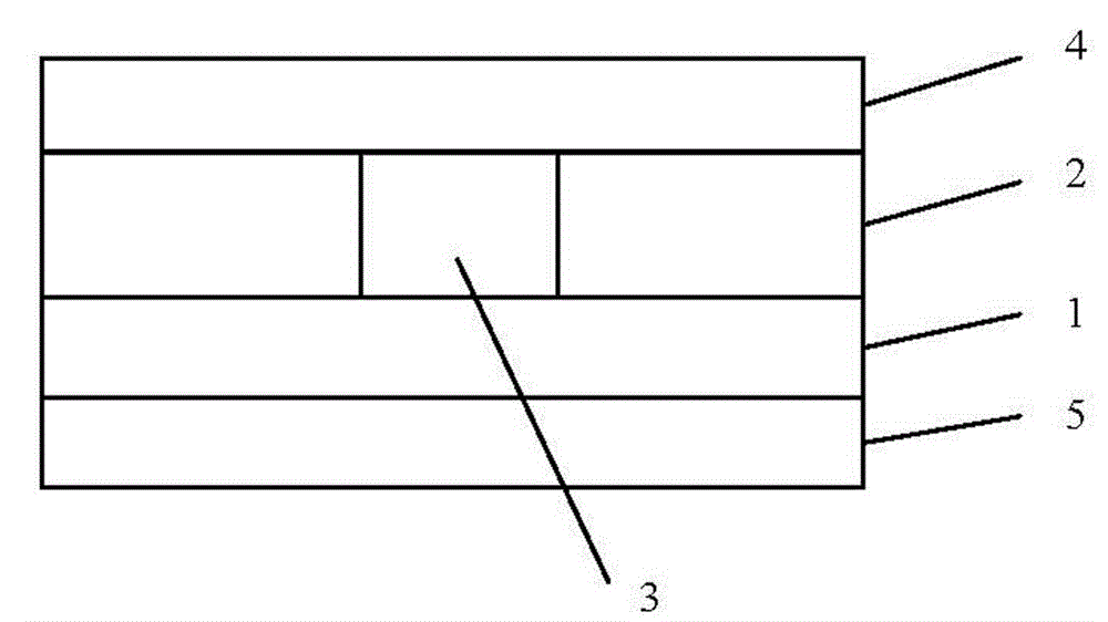
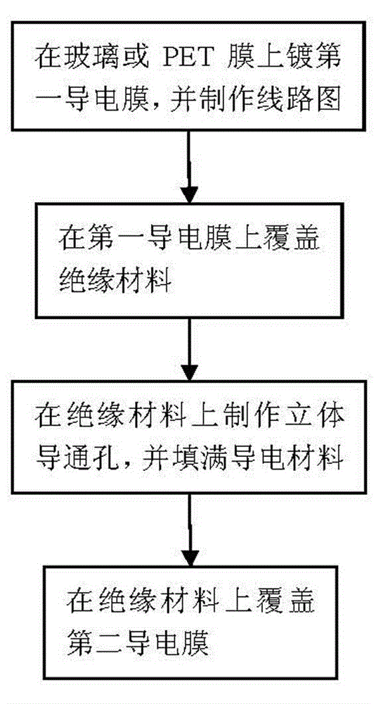
[0015] Such as figure 1 As shown, the capacitive touch screen with three-dimensional via holes proposed by an embodiment of the present invention includes a first conductive film layer 1 plated on a single piece of glass 5 or a PET film, and the first conductive film layer can be indium tin Oxide film or copper film, alloy film and other conductive films, which are plated on glass or PET film by sputtering or electroplating, the thickness of the material itself is very thin, which is very conducive to reducing the overall thickness of capacitive touch screen products . On the first conductive film layer, an insulating layer 2 and a second conductive film layer 4 are successively arranged, and the material used for the insulating layer is a photosensitive or non-photosensitive insulating substance, such as photosensitive or non-photosensitive insulating black ink, insulating white ink or Insulating oil (UV), etc., make the insulating layer very thin. The second conductive film...


PUM


Abstract

The invention discloses a capacitive control screen with a three-dimensional via hole and a manufacturing method thereof. The capacitive control screen comprises a first conducting film layer plated on glass or a PET (polyethylene terephthalate) film, and an insulating layer and a second conducting film layer which are sequentially arranged on the first conducting film layer, the first conducting film layer and the second conducting film layer are provided with corresponding circuits, the insulating layer is provided with a via hole, and a conducting medium used for conducting the circuits is filled in the via hole. According to the capacitive control screen disclosed by the invention, the via hole is manufactured in the insulating layer without damaging the conducting films, so that the manufacturing process of the capacitive control screen is greatly improved.

Description

technical field [0001] The invention relates to the field of capacitive control panels, in particular to a capacitive control panel with three-dimensional via holes and a manufacturing method thereof. Background technique [0002] The structure of the double-sided circuit board is that there is an insulating layer between the upper and lower wire layers, and the via hole is mainly used between the two layers and the wire layer, and plays the role of conducting and connecting the upper and lower wire layers. [0003] The commonly used method of making via holes in the industry is to directly punch holes on double-sided circuit boards, and then inject conductive medium to form via holes. This method is easy to damage the circuit board, especially when the circuit board needs to be bent, the conduction The hole position is prone to brittle fracture. Especially in the process of capacitive control panels with high requirements for thin thickness and precision, it is extremely d...

Claims


Application Information

Patent Timeline
Patent Type & Authority Applications(China)
IPC IPC(8): G06F3/044
Inventor 赵继虎
Owner 宏科有限公司
Why Eureka
Try Eureka