Parallel Synthesis Method and System for Integrated Circuit Design

A technology of integrated circuits and synthesis methods, applied in the field of parallel synthesis methods and systems, can solve the problems of inability to generate circuits, not taking into account the various deformation structures of CDFG at the same time, and long computer running time, etc., to achieve the effect of shortening the time.

Active Publication Date: 2016-08-10
SHANGHAI ANLOGIC INFOTECH CO LTD
View PDF2 Cites 0 Cited by
  • Summary
  • Abstract
  • Description
  • Claims
  • Application Information

AI Technical Summary

Problems solved by technology

[0004] The inventors of the present invention have found that such a loop optimization process often requires multiple loops to meet the design goals, which takes a long time to run the computer and seriously affects the efficiency of integrated circuit hardware design
And since each cycle is locally optimized on a specific CDFG structure, there is no global consideration of multiple deformation structures of CDFG at the same time, and multiple cycles cannot produce the best circuit.

Method used


Image

  • Parallel Synthesis Method and System for Integrated Circuit Design
  • Parallel Synthesis Method and System for Integrated Circuit Design
  • Parallel Synthesis Method and System for Integrated Circuit Design

Examples


Embodiment Construction

[0032] In the following description, many technical details are proposed in order to enable readers to better understand the application. However, those skilled in the art can understand that without these technical details and various changes and modifications based on the following implementation modes, the technical solution claimed in each claim of the present application can be realized.

[0033] In order to make the purpose, technical solution and advantages of the present invention clearer, the following will further describe the implementation of the present invention in detail in conjunction with the accompanying drawings.

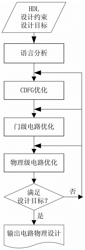
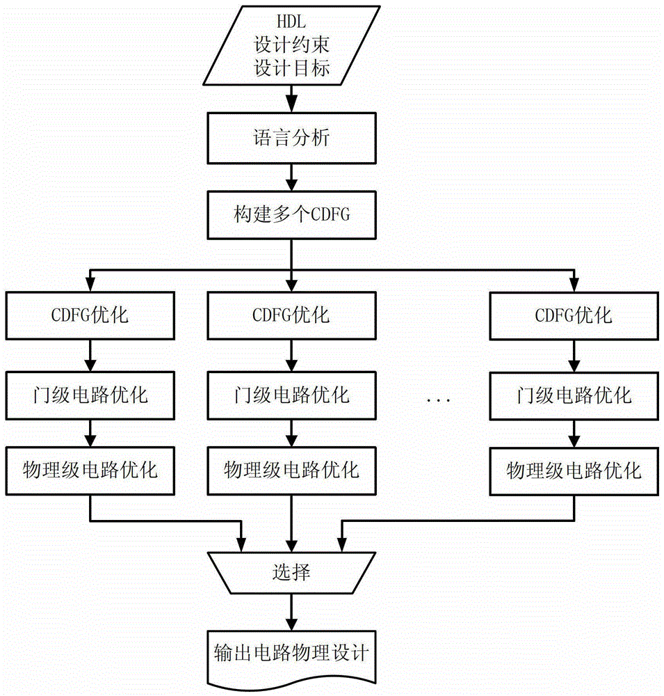
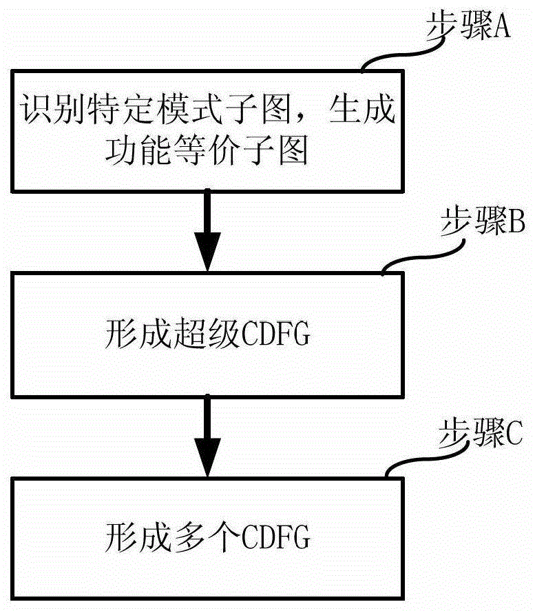
[0034] The first embodiment of the present invention relates to a parallel synthesis method for integrated circuit design. figure 2 is a flow diagram of the parallel synthesis method. The above synthesis is to transform the high-level hardware description into a low-level hardware description, such as figure 2 As shown, the method includes the...


PUM


Abstract

The invention relates to the field of integrated circuit design and discloses a parallel integration method and system for integrated circuit design. The parallel integration method comprises the steps of: simultaneously generating a plurality of functional equivalent subgraphs of specific-mode subgraphs in an original CDFG (Control Data Flow Graph) by using the parallel processing capability in a computer technology, combining the functional equivalent subgraphs of each specific-mode subgraph into a plurality of CDFGs, carrying out parallel treatment and optimization on the plurality of CDFGs, simultaneously generating a plurality of low-level hardware circuits, and finally, selecting and determining the low-level hardware circuit with the optimal performance for one time. And therefore, the integration time required by the plurality of CDFGs is only one cycle time of the traditional integration flow, the time required for integration is greatly shortened, and in addition, as the combination of all the functional equivalent subgraphs is structured into a special CDFG to be optimized independently, the optimal circuit finally determined through parallel integration via parallel search is the optimal result which can be found out in all solution spaces.

Description

technical field [0001] The invention relates to the field of integrated circuit design, in particular to a parallel synthesis method and system for integrated circuit design. Background technique [0002] Synthesis is the process of converting a high-level hardware description format into a low-level hardware description format. Register transfer level synthesis (RTL Synthesis) is the process of converting a register transfer level circuit described in a hardware description language (Hardware Description Language, "HDL") such as Verilog or VHDL into a gate level circuit with functional information. Gate-level synthesis (Gate-level Synthesis) is the process of converting a gate-level circuit with functional information into a gate-level circuit with physical information. Physical Synthesis (Physical Synthesis) is the process of determining the position of the gate-level circuit with physical information in the final physical chip and the shape of the interconnecting wires a...

Claims


Application Information

Patent Timeline
Patent Type & Authority Patents(China)
IPC IPC(8): G06F17/50
Inventor 王元陈利光赵永胜徐春华
Owner SHANGHAI ANLOGIC INFOTECH CO LTD
Why Eureka
Try Eureka