Encapsulation method for semiconductor laser array
A packaging method and semiconductor technology, applied in the direction of semiconductor lasers, lasers, laser components, etc., can solve the problems of high power density waste heat, limit the application and operation reliability of semiconductor lasers, etc.
- Summary
- Abstract
- Description
- Claims
- Application Information
AI Technical Summary
Problems solved by technology
Method used
Image
Examples
Embodiment Construction
[0019] In order to clearly illustrate the technical characteristics of this solution, the following describes this solution through a specific implementation mode combined with its accompanying drawings.
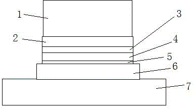
[0020] It can be seen from the attached drawings that the packaging method of the semiconductor laser line array of this scheme is as follows:
[0021] a. Fabrication of insulating films on microchannel coolers;
[0022] b. Prepare solder on the insulating film;
[0023] c. Fixing the semiconductor chip and the microchannel cooler using a jig assembly;
[0024] d. welding the semiconductor chip on the insulating film;
[0025] e. Pressure welding electrode leads.
[0026] Wherein the thickness of the insulating film is 1nm-500nm; the insulating film is a metal oxide film.
[0027] The fixture in step c includes a press block, a bead and a base; the weight of the bead is 5-500 grams; the size of the bead is equal to the size of the semiconductor chip, the thickness of the...
PUM
| Property | Measurement | Unit |
|---|---|---|
| Thickness | aaaaa | aaaaa |
| Thickness | aaaaa | aaaaa |
Abstract
Description
Claims
Application Information
