High-dielectric-constant metal gate production method

A high dielectric constant, metal gate technology, applied in semiconductor devices and other directions, can solve problems such as affecting the performance of semiconductor devices, and achieve the effect of preventing diffusion and improving performance

Active Publication Date: 2013-06-26
SEMICON MFG INT (SHANGHAI) CORP
View PDF7 Cites 4 Cited by
  • Summary
  • Abstract
  • Description
  • Claims
  • Application Information

AI Technical Summary

Problems solved by technology

[0006] In the above existing method, the deposited Al electrode 9 is easy to diffuse through the isolation layer 8 into the metal work function layer 7 or even the high dielectric constan...

Method used


Image

  • High-dielectric-constant metal gate production method
  • High-dielectric-constant metal gate production method
  • High-dielectric-constant metal gate production method

Examples


Embodiment Construction

[0024] In order to make the object, technical solution and advantages of the present invention clearer, the present invention will be further described in detail below with reference to the accompanying drawings and examples.

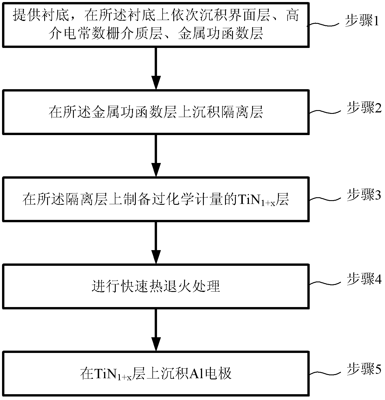
[0025] Such as image 3 shown, and refer to Figure 4 to Figure 8 , the high dielectric constant metal gate manufacturing method of the present invention, comprising:

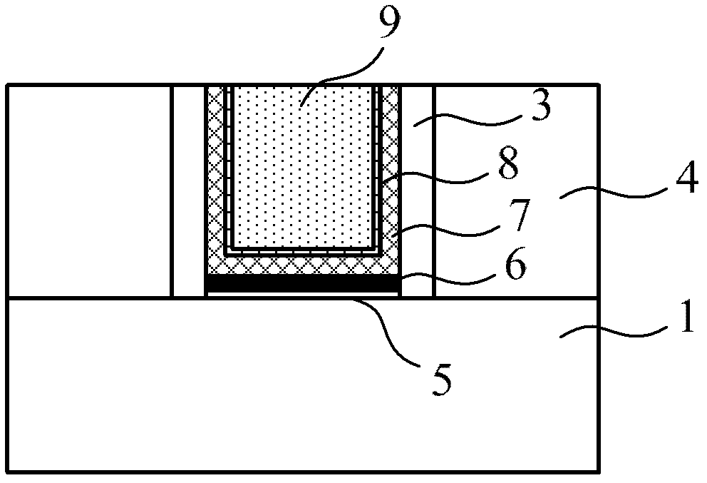
[0026] Step 1: If Figure 4 As shown, a substrate 1 is provided, and an interface layer 5 , a high dielectric constant gate dielectric layer 6 and a metal work function layer 7 are sequentially deposited on the substrate.

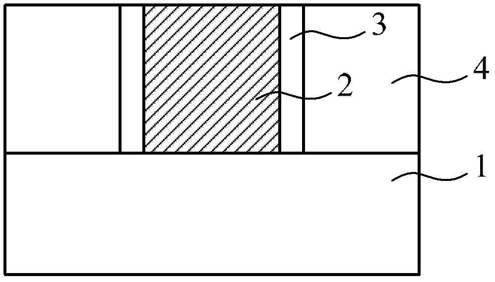
[0027] The substrate 1 may include any basic material on which a semiconductor device can be built, such as a silicon substrate, or a silicon substrate on which field isolation regions have been formed, or a silicon substrate on an insulating material.

[0028] In the prior art, other necessary steps are also included before step 1. Can refer to figure 1 and fi...


PUM

PropertyMeasurementUnit
Thicknessaaaaaaaaaa

Abstract

The invention discloses a high-dielectric-constant metal gate production method which includes that a substrate is provided, and an interface layer, a high-dielectric-constant gate medium layer and a metal work function layer are sequentially deposited on the substrate; an isolation layer is deposited on the metal work function layer; a stoichiometric TiN1+x layer is prepared on the isolation layer; rapid thermal annealing is performed; and an Al electrode is deposited on the TiN1+x layer. According to the method, after the isolation layer is deposited, the stoichiometric TiN1+x layer is prepared on the isolation layer, high-concentration solid N is diffused in the rapid thermal annealing process, accordingly the crystal boundary of crystals of the isolation layer is changed, further the route of metal Al in the Al electrode diffusing towards the metal work function layer and the high-dielectric-constant gate medium layer is destroyed, Al electrode diffusing is avoided, and performance of semiconductor devices is improved.

Description

technical field [0001] The invention relates to semiconductor manufacturing technology, in particular to a manufacturing method of a high dielectric constant metal gate. Background technique [0002] At present, on the 28nm process node, the use of HKMG (high dielectric constant metal gate) structure to replace the traditional polysilicon gate structure has been recognized as the main and only means to solve the problems of gate leakage current, polysilicon loss and boron penetration. However, in the HKMG process, many new problems are also faced, such as the problem of Al diffusion to the metal work function layer, which will affect the work function of the semiconductor device. [0003] An existing method for manufacturing metal gates refers to figure 1 and figure 2 . [0004] Such as figure 1 As shown, a substrate 1 is provided, such as an N-type or P-type substrate, on which a dummy polysilicon gate 2 formed of polysilicon is deposited, and sidewalls 3 are provided....

Claims


Application Information

Patent Timeline
IPC IPC(8): H01L21/28
Inventor 李凤莲倪景华
Owner SEMICON MFG INT (SHANGHAI) CORP
Why Eureka
Try Eureka