Wafer to wafer connection structure
A technology of bonding structure and wafer, applied in the direction of electrical components, electric solid-state devices, circuits, etc., can solve problems such as inability to align
- Summary
- Abstract
- Description
- Claims
- Application Information
AI Technical Summary
Problems solved by technology
Method used
Image
Examples
Embodiment Construction
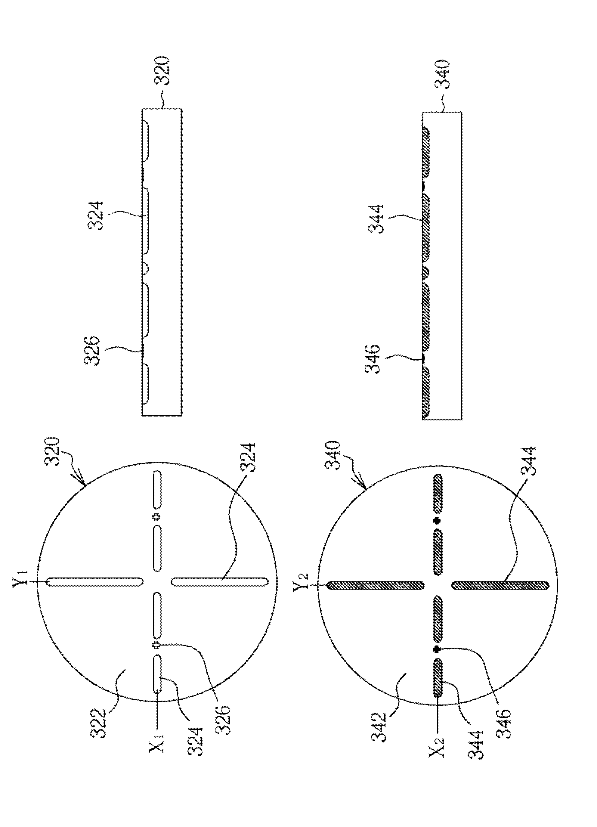
[0031] now refer to image 3 , which depicts a top view and a cross-sectional view of two first wafers and second wafers to be docked before bonding according to an embodiment of the present invention. Such as image 3 As shown, the wafer-to-wafer bonding structure of the present invention is formed by bonding a first wafer 320 and a second wafer 340 . The first chip 320 has a first surface 322 on which a plurality of first grooves 324 and various components and circuits (not shown) are disposed. In this embodiment, more than one first groove 324 may be respectively provided on the transverse diameter X1 and the longitudinal diameter Y1 of the first wafer 320 . Wherein, the first trench 324 provided on the lateral diameter X1 of the first wafer 320 has a length parallel to the lateral diameter X1 and a width parallel to the longitudinal diameter Y1, and the groove 324 provided on the longitudinal diameter Y1 of the first wafer 320 The first trench 324 has a length parallel ...
PUM
 Abstract
Description
Claims
Application Information


