Supercharge Your Innovation With Domain-Expert AI Agents!

Making method of tensile stress LPCVD SiO2 membrane

A manufacturing method and a tensile stress technology, which are applied in the manufacture of microstructure devices, processes for producing decorative surface effects, coatings, etc., can solve the problem that cannot be effectively used in the preparation process of dual-material micro-cantilever infrared focal plane arrays, thin films It is impossible to take into account the problems of stress matching and corrosion resistance, so as to achieve the effect of enhancing corrosion ability and simple process

Active Publication Date: 2013-07-03
SOI MICRO CO LTD
View PDF8 Cites 1 Cited by
  • Summary
  • Abstract
  • Description
  • Claims
  • Application Information

AI Technical Summary

Problems solved by technology

While the prior art SiO 2 The thin film preparation process cannot take into account stress matching and corrosion resistance, and cannot be effectively used in the preparation process of dual-material micro-cantilever infrared focal plane arrays

Method used


Image

  • Making method of tensile stress LPCVD SiO2 membrane
  • Making method of tensile stress LPCVD SiO2 membrane
  • Making method of tensile stress LPCVD SiO2 membrane

Examples


Embodiment Construction

[0028] The characteristics and technical effects of the technical solution of the present invention will be described in detail below with reference to the accompanying drawings and in conjunction with schematic embodiments, and a tensile stress LPCVD SiO with both stress matching and corrosion resistance is disclosed. 2 Film manufacturing method. It should be pointed out that similar reference numerals represent similar structures, and the terms "first", "second", "upper", "lower" and the like used in this application can be used to modify various device structures or manufacturing processes . These modifications do not imply spatial, sequential or hierarchical relationships of the modified device structures or fabrication processes unless specifically stated.

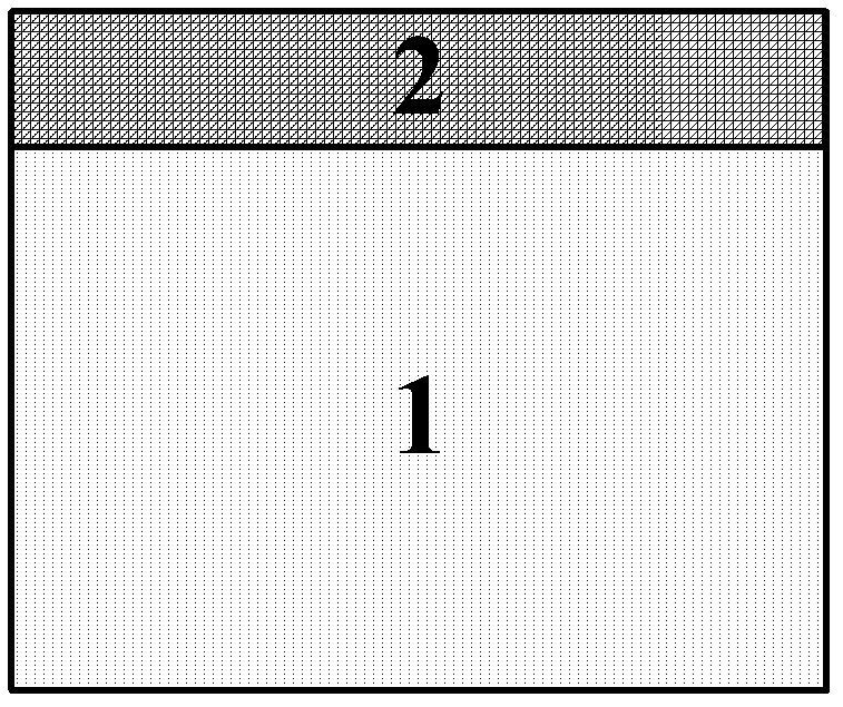
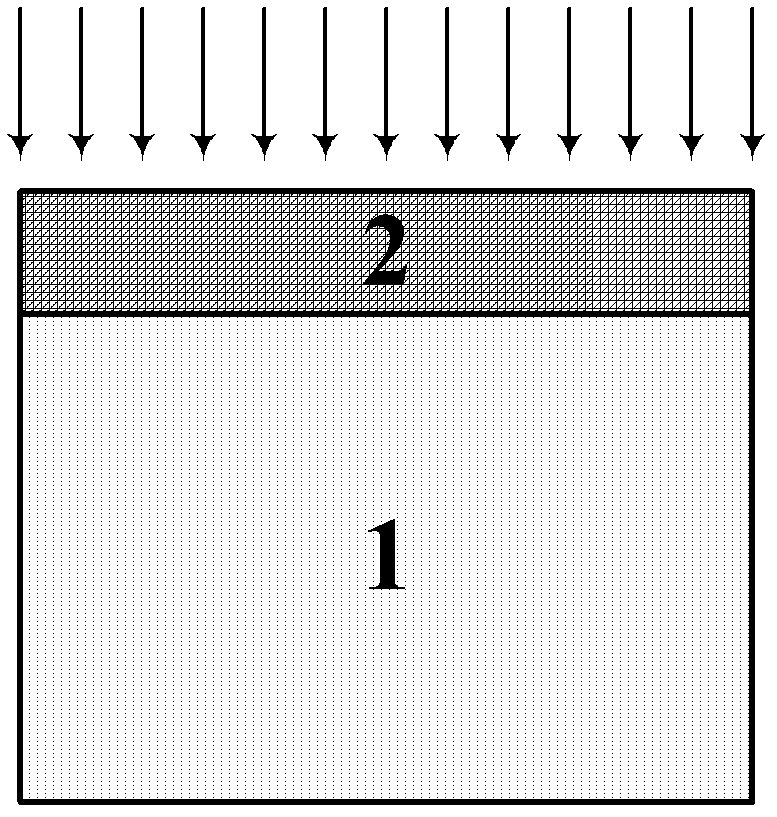
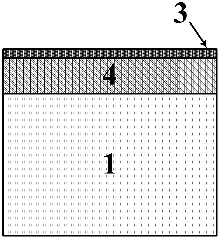
[0029] The invention provides a tensile stress LPCVD SiO 2 The manufacturing method of thin film, its flow process refers to Figure 1 to Figure 3 , its specific process steps are as follows:

[0030] Step S1, usi...


PUM


Abstract

The invention discloses a making method of a tensile stress LPCVD (low pressure chemical vapor deposition) SiO2 membrane. The method includes: depositing a compressive stress SiO2 membrane with stress of F1 on a substrate by LPCVD, with the F1 less than 0; injecting a dopant into the compressive stress SiO2 membrane to form a heavily doped SiO2 membrane on its surface; and conducting annealing to convert the compressive stress SiO2 membrane to the tensile stress SiO2 membrane with stress of F2 greater than 0. The making method of the LPCVD tensile stress SiO2 membrane has a simple process, is compatible with traditional microfabrication processes, not only realizes stress matching of a bimaterial cantilever beam, but also significantly enhances the corrosion resistance of SiO2 to XeF2, and finally makes making of the bimaterial and stress matched cantilever beam that adopts Al and SiO2 come true successfully.

Description

technical field [0001] The invention relates to a method for manufacturing a semiconductor device, in particular to a tensile stress LPCVD SiO 2 Membrane manufacturing method. Background technique [0002] With the rapid development of vacuum science technology, optoelectronic technology and semiconductor technology, thin-film optical devices and thin-film electronic devices have been widely used. In the optical readout uncooled infrared focal plane imaging system based on the micro-cantilever array structure of MEMS, its core structure is the uncooled infrared detector system, that is, the dual-material micro-cantilever infrared focal plane array (FPA), which consists of a series of The imaging pixels form an areal array, and each pixel is composed of two materials with very different thermal expansions. The pixel converts the radiation energy into heat energy by absorbing the infrared radiation of the object, and converts the heat energy into the rotation angle or displa...

Claims


Application Information

Patent Timeline
Patent Type & Authority Applications(China)
IPC IPC(8): B81C1/00
Inventor 尚海平焦斌斌刘瑞文陈大鹏李志刚卢迪克
Owner SOI MICRO CO LTD
Features
  • R&D
  • Intellectual Property
  • Life Sciences
  • Materials
  • Tech Scout
  • Unparalleled Data Quality
  • Higher Quality Content
  • 60% Fewer Hallucinations
Learn More