Switch circuit

一种开关电路、开关元件的技术,应用在电子开关、电气元件、脉冲技术等方向,能够解决电路规模变大、电路结构复杂等问题

Active Publication Date: 2013-07-03
MURATA MFG CO LTD
View PDF6 Cites 1 Cited by
  • Summary
  • Abstract
  • Description
  • Claims
  • Application Information

AI Technical Summary

Problems solved by technology

However, there is a problem that the circuit scale becomes larger and the circuit structure is complicated.

Method used


Image

  • Switch circuit
  • Switch circuit
  • Switch circuit

Examples


Embodiment approach 1

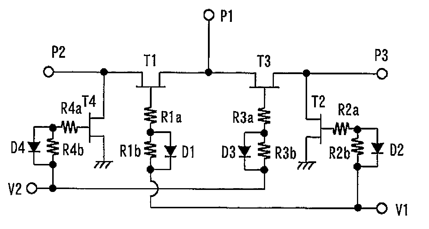
[0034] FIG. 1 is a diagram showing a switch circuit according to Embodiment 1 of the present invention. The transistors T1, T2, T3, T4 are field effect transistors used as switching elements. The control voltage application terminals V1 and V2 are terminals for applying a control voltage for switching the switches. The resistors R1a, R1b, R2a, R2b, R3a, and R4a are isolation resistors of several kΩ or more connected to the gates of the respective transistors.

[0035] The transistor T1 is connected between the input / output terminal P1 and the input / output terminal P2. The transistor T2 is connected between the input / output terminal P3 and a ground point. The transistor T3 is connected between the input / output terminal P1 and the input / output terminal P3. The transistor T4 is connected between the input / output terminal P2 and a ground point. The control voltage application terminal V1 is connected to the gates of the transistors T1 and T2. The control voltage application t...

Embodiment approach 2

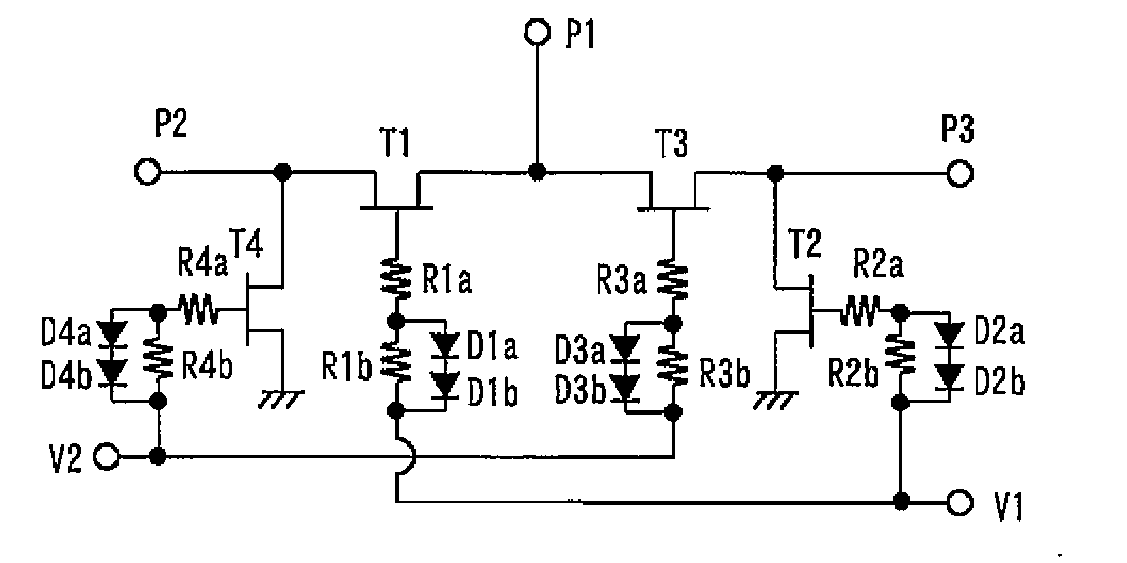
[0055] FIG. 7 is a diagram showing a switch circuit according to Embodiment 2 of the present invention. In addition to the configuration of Embodiment 1, resistors R3b, R4b are connected between the gates of transistors T3, T4 and control voltage application terminal V2, respectively. Diodes D3, D4 are connected in parallel to resistors R3b, R4b, respectively, and the cathodes of diodes D3, D4 are connected to control voltage application terminal V2.

[0056] In the present embodiment, a diode is arranged in parallel with a part of the gate resistors of the transistors in both paths of the switch. When this switch circuit is used in the system shown in FIG. 18, the power withstand performance against high-power signals from a plurality of antennas at the time of reception is improved. As a result, it is possible to prevent a decrease in signal switching accuracy caused by the switching circuit.

[0057] FIG. 8 is a diagram showing a modified example of the switching circuit ...

Embodiment approach 3

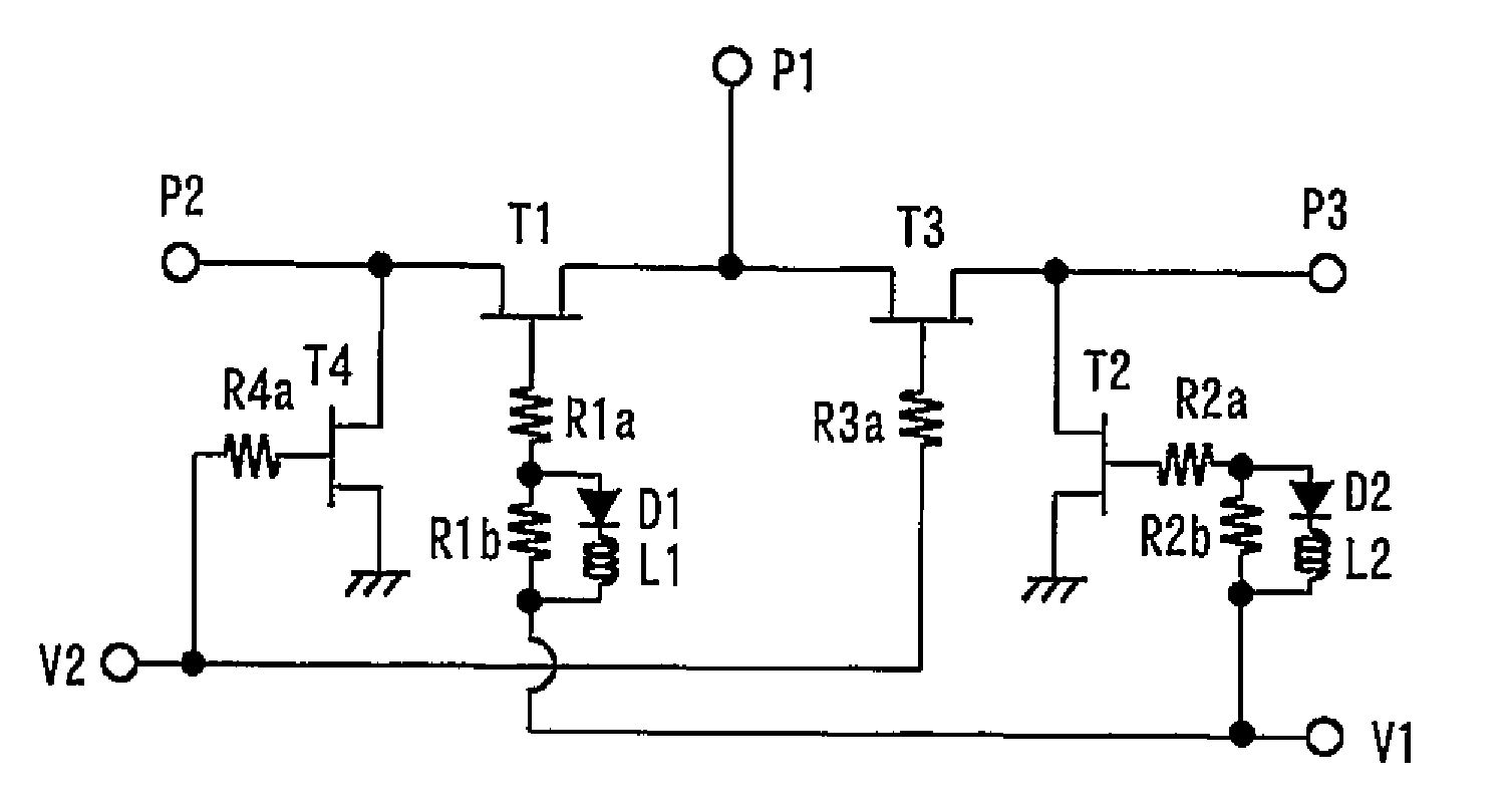
[0059] FIG. 9 is a diagram showing a switch circuit according to Embodiment 3 of the present invention. In addition to the configuration of Embodiment 1, choke inductors L1, L2 are connected in parallel to resistors R1b, R2b, respectively, and are connected in series to diodes D1, D2, respectively. Here, the gate current flows through the diodes D1, D2, and the resistors R1b, R2b connected in parallel are short-circuited. The choke inductors L1 and L2 prevent the impedance drop at this time, so the isolation function can be maintained.


PUM


Abstract

A switch circuit includes: first, second, and third input-output terminals; a transistor (T1) connected between the first and second input-output terminals (P1) and (P2); a transistor (T2) connected between the third input-output terminal (P3) and a grounding point; a transistor (T3) connected between the first and third input-output terminals (P1) and (P3); a transistor (T4) connected between the second input-output terminal (P2) and the grounding point; a first control voltage applying terminal (V1) connected to control terminals of the first and second switching elements (T1) and (T2) ; a second control voltage applying terminal transistor (V2) connected to control terminals of the third and fourth switching elements (T3) and (T4); first and second resistors (R1b, R2b) connected between the control terminals of the first and second switching elements (T1) and (T2) and the first control voltage applying terminal (V1), respectively; and first and second diodes (D1, D2) connected in parallel with the first and second resistors (R1b, R2b), respectively, and having cathodes connected to the first control voltage applying terminal (V1).

Description

technical field [0001] The present invention relates to switching circuits mainly used in high-band wireless communication equipment, high-band radar equipment, and the like. Background technique [0002] Switching circuits are used in systems that transmit signals in high frequency bands such as microwave bands and millimeter wave bands. 17 , 18 and 19 are diagrams showing a system using a switching circuit. [0003] The switch SW is used for switching between transmission and reception of signals in FIG. 17 . The switch SW is used for switching the signals from the two antennas ANT in FIG. 18 . In FIG. 19, when a relatively high power signal is transmitted from the transmitter S1 in the system using the circulator CIR, the switch SW is used to prevent the signal from being reflected from the antenna ANT and input to the receiver J1. Thus, the receiver J1 including the low noise amplifier can be protected. In these systems, a switching circuit in which switching element...

Claims


Application Information

Patent Timeline
Patent Type & Authority Applications(China)
IPC IPC(8): H03K17/687
CPCH03K17/693
Inventor 塚原良洋
Owner MURATA MFG CO LTD
Why Eureka
Try Eureka