Wafer testing method used for design analysis purpose

A technology of wafer testing and design analysis, applied in the field of wafer testing, can solve problems such as poor needle stability, damaged chips, unstable signals, etc., and achieve the effect of improving the efficiency of detection signals

Inactive Publication Date: 2013-07-10
XI AN UNIIC SEMICON CO LTD
View PDF10 Cites 7 Cited by
  • Summary
  • Abstract
  • Description
  • Claims
  • Application Information

AI Technical Summary

Problems solved by technology

This process can take hours and even risk damaging the chip
And changing the probe card means changing the test conditions. For different probe cards, there are different winding methods and lengths. It is very likely that the test results will not be comparable under certain conditions.
[0007] Even if different probe cards are used, since the pins on the probe card must be in good contact with the bonding pad (pad) to ensure the normal operation of the chip, the active area of ​​the opening and the micro-probe is very limited, and it must be ensured that it does not contact the probe. When

Method used


Image

  • Wafer testing method used for design analysis purpose
  • Wafer testing method used for design analysis purpose
  • Wafer testing method used for design analysis purpose

Examples


Embodiment Construction

[0030] Below in conjunction with accompanying drawing, content of the present invention is elaborated:

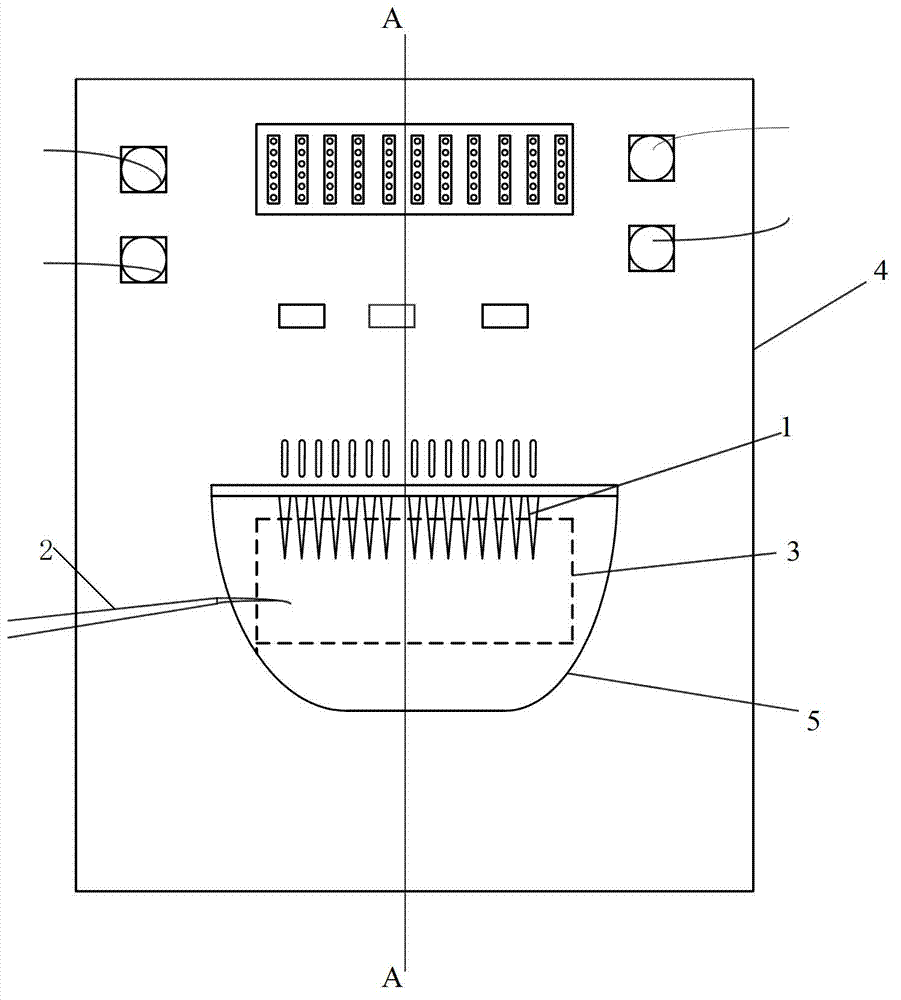
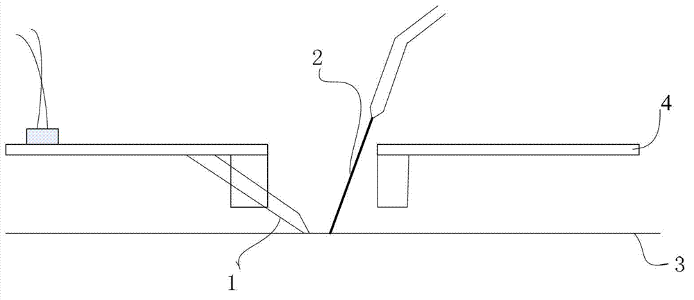
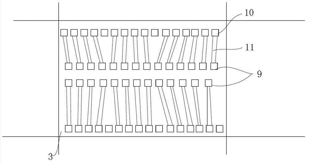
[0031] refer to image 3 , the present invention provides a wafer test method for design and analysis purposes, a redistribution layer 13 is made on the finished wafer, and some first pads of chips in the wafer are connected to the redistribution layer through the redistribution layer connecting wires. Several second pads corresponding to the first pads on the layer are connected, and the second pads of the redistribution layer 13 are located outside the area probed by the microprobe, for example: a position that does not need to be probed inside the chip, or between a chip and a chip. In between, or near the top of the chip, use the probe card to test the wafer at the second pad position of the redistribution layer, and use the micro-probe on the chip to perform signal testing on the chip. The needles of the card are separated, thereby effectively increasing the contact a...


PUM


Abstract

The invention provides a wafer testing method used for a design analysis purpose. A redistribution layer is manufactured on the surface of a manufactured wafer, a plurality of first pads of a chip of the wafer are connected with a plurality of second pads which are located on the redistribution layer and correspond to the first pads through redistribution layer connecting wires, the second pads on the redistribution layer are located outside the area detected by a microprobe, testing stimuli are inflicted in the positions of the second pads on the redistribution layer with a probe of a probe card, signal testing is carried out on the chip with the microprobe, the probe of the probe card and the microprobe are separated physically, and the probe of the probe card and the microprobe are not affected by each other. The wafer testing method used for the design analysis purpose widens the range of the contact of the microprobe and chip to the maximum, ensures that the signal testing can be carried out normally and obviously promotes efficiency of detecting signals.

Description

technical field [0001] The invention relates to the field of semiconductor design and testing, in particular to a wafer testing method for design and analysis purposes. Background technique [0002] In the development stage of large-scale integrated circuits, it is very important to perform verification analysis on the initially produced circuits. Only after the first batch of wafer process is completed, it is possible to verify whether the simulation model is correct and whether the chip is working properly, and it is possible to conduct more extensive tests under different conditions to find the weak link of the chip design. Because of this, the first batch of wafers will be tested more extensively than later mature wafers, some specific analytical instruments and devices will be used, and even the process and standards of the first batch of wafers will be different, such as ML wafer (ML wafer technical term, refers to the metal layer on the wafer surface) and PT wafer (P...

Claims


Application Information

Patent Timeline
IPC IPC(8): G01R31/28
Inventor 张涛郝福亨
Owner XI AN UNIIC SEMICON CO LTD
Why Eureka
Try Eureka