Shifting register and gate driving circuit and repairing method and display device thereof

A gate drive circuit, shift register technology, applied in static memory, digital memory information, instruments, etc., can solve the problem that the shift register cannot work

Inactive Publication Date: 2013-07-10
BOE TECH GRP CO LTD
View PDF5 Cites 20 Cited by
  • Summary
  • Abstract
  • Description
  • Claims
  • Application Information

AI Technical Summary

Problems solved by technology

[0005] Embodiments of the present invention provide a shift register, a gate drive circuit, a repair method thereof, and a display device to solve the problem that an existing GOA circuit cannot work due to a fault in a shift register

Method used


Image

  • Shifting register and gate driving circuit and repairing method and display device thereof
  • Shifting register and gate driving circuit and repairing method and display device thereof
  • Shifting register and gate driving circuit and repairing method and display device thereof

Examples


Embodiment 1

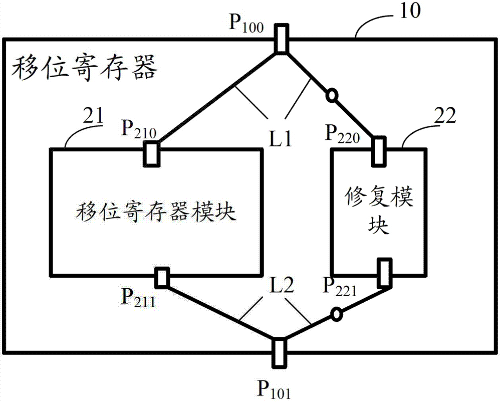
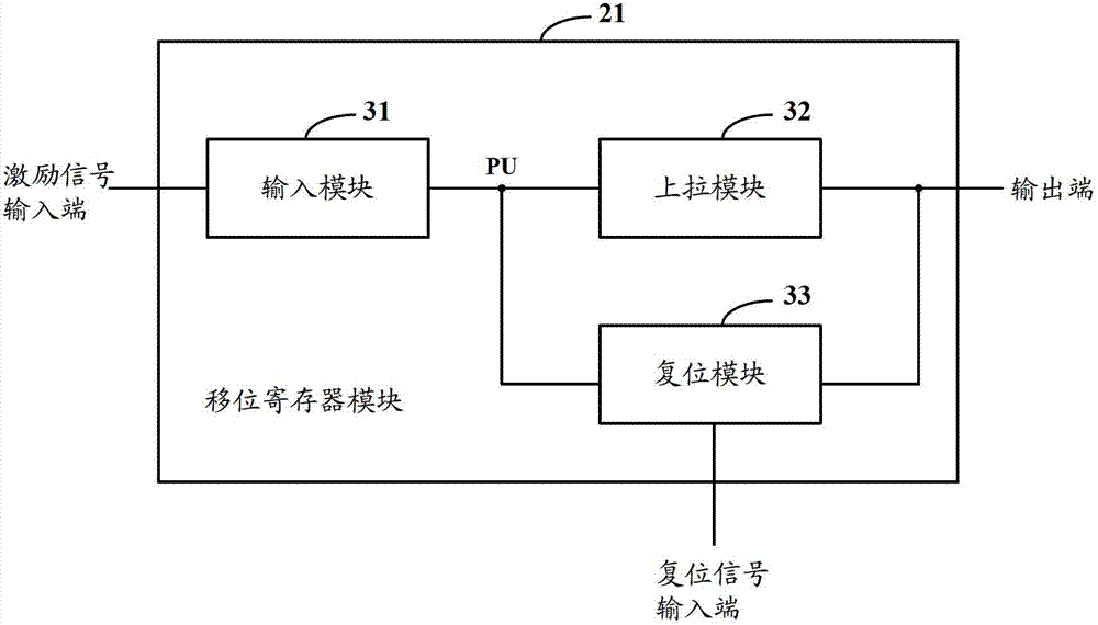
[0031] Such as figure 1 As shown, it is a shift register 10 in Embodiment 1 of the present invention, and the shift register 10 includes: a first connectable link L1, a second connectable link L2, an excitation signal input terminal P 100 , output terminal P 101 and the first clock signal input ( figure 1 Not shown in), and the shift register module 21 and the repair module 22; the shift register module 21 includes an excitation signal input terminal P 210 , output terminal P 211 and the first clock signal input terminal ( figure 1 not shown in); the repair module 22 includes an excitation signal input terminal P 220 and the output P 221 ;in:

[0032] The first connectable link L1 is set at the excitation signal input terminal P of the shift register 10 100 , the excitation signal input terminal P of the shift register module 21 210 and the excitation signal input terminal P of the repair module 22 220 Between, when the shift register module 21 breaks down, disconnect...

Embodiment 2

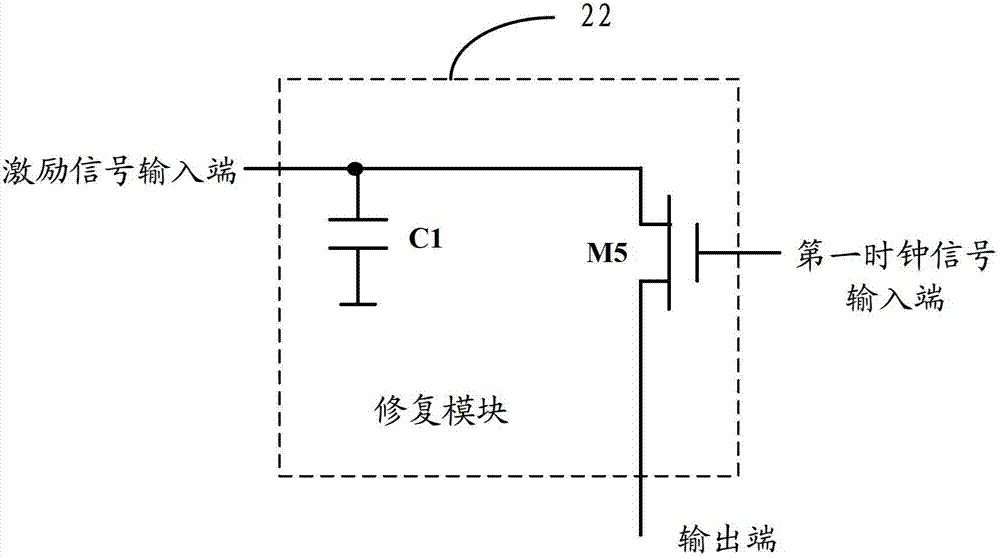
[0042] On the basis of Embodiment 1 of the present invention, a shift register is provided in Embodiment 2 of the present invention, and the circuit implementing the function of the repair module in the shift register is specifically limited. The circuit diagram of the repair module 22 of the shift register Such as figure 2 As shown, including: a first capacitor C1 and a fifth transistor M5;

[0043] One end of the first capacitor C1 is connected to the excitation signal input end of the repair module, and the other end is grounded;

[0044] The gate of the fifth transistor M5 is connected to the first clock signal input terminal, the first pole is connected to the excitation signal input terminal of the repair module, and the second pole is connected to the output terminal of the repair module. It can be understood that, for example, the first clock signal input terminal connected to the gate of the fifth transistor M5 may be the first clock signal input terminal of the shi...

Embodiment 3

[0093] Embodiment 3 of the present invention provides a gate drive circuit, the schematic diagram of which is shown in Figure 7 As shown, the gate drive circuit includes a plurality of shift registers as described in any one of the third embodiment, wherein:

[0094] Except for the first shift register and the last shift register, the output terminal of each other shift register and the reset signal input terminal of the upper stage shift register adjacent to it and the next stage shift register adjacent to it The excitation signal input end of the register is connected, and the gate drive circuit sequentially outputs the signals output by the output ends of the shift registers at all levels;

[0095] The output end of the first shift register is connected to the excitation signal input end of the second shift register, and the output end of the last shift register is connected to the reset signal input end of the previous shift register adjacent to it;

[0096] The excitati...


PUM


Abstract

The invention discloses a shifting register and a gate driving circuit and a repairing method and a display device of the shifting register and the gate driving circuit. The shifting register comprises a shifting register module, a repairing module, a first connection link and a second connection link, wherein the first connection link and the second connection link are arranged between the shifting register module and the repairing module and are used for switching on or off output ends and input ends of the shifting register module and the repairing module, the shifting register module is used for outputting clock signals input from a first clock signal input end through an output end of the shifting register module according to excitation signals received from an excitation signal input end of the shifting register module, and the repairing module is used for delaying the excitation signals received from an excitation signal input end of the repairing module for a half clock period and outputs the excitation signals from an output end of the repairing module when the shifting register module fails. Due to the fact that the shifting register is provided with the repairing module with the functions to replace the shifting register module, the subsequent work of the shifting register is not affected when the shifting register module fails.

Description

technical field [0001] The invention relates to the field of flat panel display technology, in particular to a shift register, a gate drive circuit, a repair method thereof, and a display device. Background technique [0002] Flat panel display is developing rapidly because of its ultra-thin energy saving. Shift registers are used in most flat-panel displays. At present, shift registers realized by Gate on Array (GOA) technology can not only be integrated on the gate drive integrated circuit, but also reduce the production of a display panel. The process, therefore, saves cost, so in recent years, GOA technology has been widely used in the flat panel display manufacturing process. [0003] The current problem of using GOA technology is that the shift register of GOA depends on the output signal of the upper-stage shift register, and the output signal of the upper-stage shift register is used as the input signal of the current-stage shift register. The output signal of the ...

Claims


Application Information

Patent Timeline
Patent Type & Authority Applications(China)
IPC IPC(8): G09G3/20G11C19/28
CPCG11C19/184G11C19/28G09G3/20G09G2310/0267G09G2310/0286G09G2330/08G09G3/007G09G2300/0426G09G2300/043G09G2310/08
Inventor 梁逸南
Owner BOE TECH GRP CO LTD
Why Eureka
Try Eureka