Method for making a step formwork

A production method and step technology are applied in the preparation of printing surface, the photoengraving process of pattern surface, printing and other directions, which can solve the problems of high cost, high energy consumption, rough spots, etc., and achieve good opening quality and high position accuracy. Effect

Inactive Publication Date: 2017-03-15
KUN SHAN POWER STENCIL
View PDF6 Cites 0 Cited by
  • Summary
  • Abstract
  • Description
  • Claims
  • Application Information

AI Technical Summary

Problems solved by technology

However, the opening precision of the steel mold made by the traditional technology through laser cutting technology cannot meet the requirements, and the quality of the board surface is not high enough.
However, the electroformed nickel mask has defects such as easy formation of pinholes and rough spots on the surface, unstable solution, high cost, and high energy consumption.

Method used


Image

  • Method for making a step formwork
  • Method for making a step formwork
  • Method for making a step formwork

Examples


Embodiment Construction

[0070] Embodiments of the present invention are described in detail below, examples of which are shown in the drawings, wherein the same or similar reference numerals designate the same or similar elements or elements having the same or similar functions throughout. The embodiments described below by referring to the figures are exemplary only for explaining the present invention and should not be construed as limiting the present invention.

[0071] The specific technological process of this legal name and the attention problem in technological process among the present invention will be more detailed in the following narration.

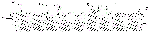
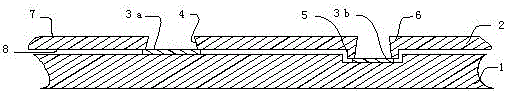
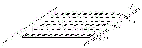
[0072] A method for making a step formwork. Its specific technological process is as follows:

[0073] (1) Choose one of stainless steel, pure nickel, and nickel-iron alloy as the substrate material, and cut the substrate into the required size;

[0074] (2) After the cut metal sheet is pickled and polished, sandblasting is performed on both sides t...


PUM


Abstract

A production method for a step stencil and the specific process flow of the method is as follows: substrate processing (cutting)->pre-treatment (degreasing, pickling, and sandblasting)->film mounting->double sided exposure->double sided developing->etching (up step areas on a PCB surface, and a printing surface)->film stripping->pre-treatment (degreasing and pickling)->laser cutting (flat openings and openings of the up step areas). By using the method, a metal stencil having up step areas on the PCB surface and the printing surface can be produced. The pattern area of the metal stencil has good opening quality, smooth hole walls, no undesirable phenomena such as blurs or jags; the position alignment precision of the opening pattern area is high; and the thickness uniformity is good, with uniformity COV less than 10%.

Description

technical field [0001] The invention relates to a method for manufacturing a stepped template, which belongs to the field of material manufacturing and processing, and in particular to a manufacturing process of a printing mask with raised steps (up steps) on both the PCB surface and the printing surface in the PCB manufacturing field. Background technique [0002] With the rapid development of my country's electronics industry, stencil printing technology has also been applied in the electronics manufacturing industry, and SMT printing is a typical example. To solder electronic components and PCBs in the manufacturing process of electronic products, tin needs to be placed on the PCB first, and there are hundreds of pads on the PCB that need to be tinned, and the position of each pad corresponds to the electronic component , the best way to accurately tin the pads that need to be tinned at one time is to print. The usual method used in the electronics manufacturing industry...

Claims


Application Information

Patent Timeline
Patent Type & Authority Patents(China)
IPC IPC(8): B41C1/12B41N1/04B41N3/03G03F7/00
Inventor 魏志凌高小平王峰周铮
Owner KUN SHAN POWER STENCIL
Why Eureka
Try Eureka