

A production process for a step stencil by using an electroforming method
A manufacturing process and step technology, which is applied in the field of material manufacturing and processing, can solve the problems of high bonding force and reduced lifespan, and achieve the effect of high bonding force, smooth hole wall, and good thickness uniformity
- Summary
- Abstract
- Description
- Claims
- Application Information
AI Technical Summary
Problems solved by technology
Method used
Image

Examples
Embodiment Construction
[0084] Embodiments of the present invention are described in detail below, examples of which are shown in the drawings, wherein the same or similar reference numerals designate the same or similar elements or elements having the same or similar functions throughout. The embodiments described below by referring to the figures are exemplary only for explaining the present invention and should not be construed as limiting the present invention.
[0085] The specific technological process of this legal name and the attention problem in technological process among the present invention will be more detailed in the following narration.
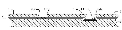
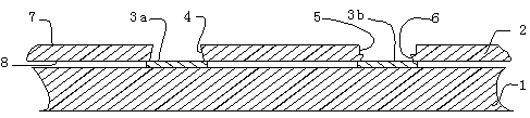
[0086] The specific process flow of the template with an up step area on the electroformed PCB surface and a down step area on the printing surface is as follows:
[0087] (1) The first electroforming layer of electroforming:
[0088] a. Mandrel processing: choose 1.8mm stainless steel as the mandrel, and cut the substrate to the required size;
...
PUM
 Abstract
Description
Claims
Application Information