Semiconductor Device And Process For Producing Semiconductor Device

A device manufacturing method and semiconductor technology, applied in the direction of semiconductor/solid-state device manufacturing, semiconductor devices, semiconductor/solid-state device components, etc., can solve problems such as product reliability decline

Active Publication Date: 2013-07-17
FUJITSU LTD
View PDF7 Cites 7 Cited by
  • Summary
  • Abstract
  • Description
  • Claims
  • Application Information

AI Technical Summary

Problems solved by technology

If the crack will extend to the product area, the reliability of the product will decrease

Method used


Image

  • Semiconductor Device And Process For Producing Semiconductor Device
  • Semiconductor Device And Process For Producing Semiconductor Device
  • Semiconductor Device And Process For Producing Semiconductor Device

Examples


example 1

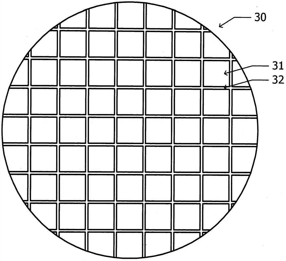
[0014] Figure 1A is a plan view showing a semiconductor wafer (30) used for the semiconductor device of Example 1. For example, a silicon wafer is used as the semiconductor wafer (30). On the surface of a semiconductor wafer (30), a plurality of product areas (chip areas) (31) arranged in a matrix are defined. Between each product area (31), a dicing area (32) is secured. The planar shape of the scribe area is a square dot matrix.

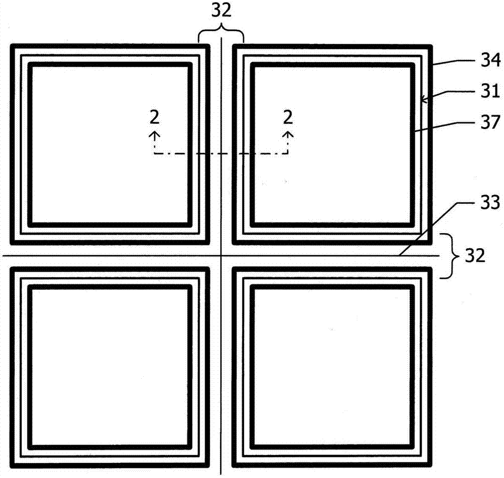
[0015] Figure 1B is a plan view showing some product areas (31 ) and some scribe areas (32). In the product area (31), a moisture-proof ring (37) is formed, and in the scribe area (32), a crack protection ring (34) is formed. Each crack protection ring (34) is arranged for each product zone (31) and surrounds the corresponding product zone (31). The planar shape of each product area (31) is rectangular or square, and the crack protection ring (34) includes a straight line extending parallel to each side of each product area (31). Each moist...

example 2

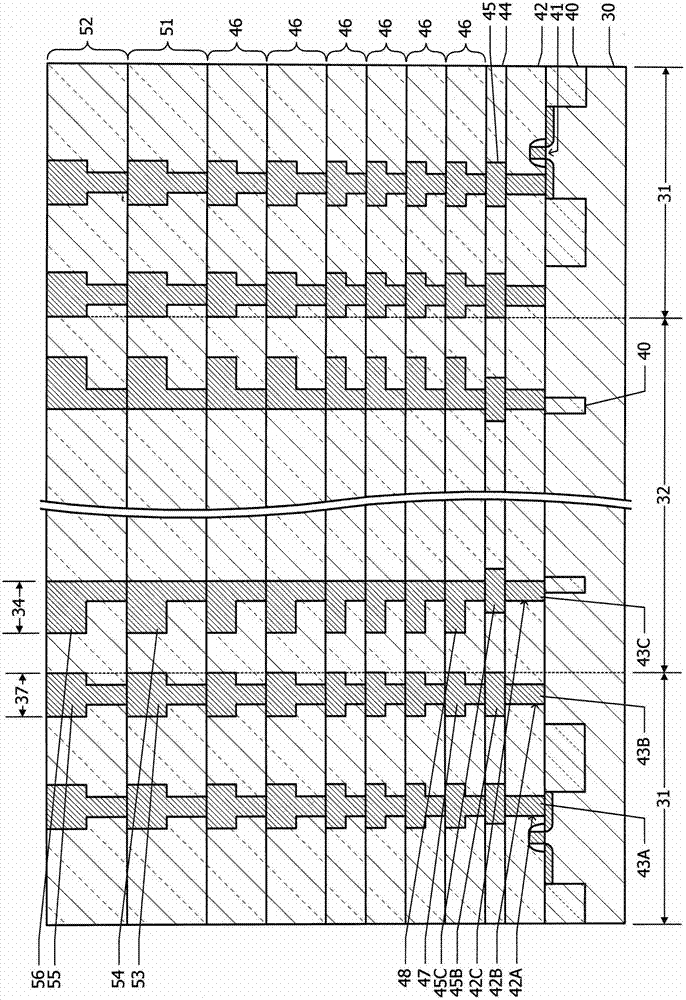
[0067] Figure 20 is a cross-sectional view showing the semiconductor device of Example 2 during the manufacturing process. Figure 20 The structure shown in Example 1 corresponds to the Figure 5 The structure of the steps shown in . In Example 1, one crack protection ring (34) is formed for each product area (31). In Example 2, outside the crack guard ring (34), a second crack guard ring (110) is formed to surround the crack guard ring (34) in plan view. The layered structure of the crack protection ring (110) is the same as that of the crack protection ring (34) on the inner peripheral side. That is, the crack guard ring (110) includes a metal film (114) in the wiring layer (52). Over the metal film (114), a metal film (113) functioning as an etching mask is arranged.

[0068] Grooves (111) and (112) are formed on the inner peripheral side and the outer peripheral side of the crack protection ring (110), respectively. Grooves ( 111 ) and ( 112 ) are formed in the same...


PUM


Abstract

A semiconductor device includes: a substrate in which a product region and scribe regions are defined; a 1st insulation film formed above the substrate; a metal film in the 1st insulation film, disposed within the scribe regions in such a manner as to surround the product region; a 2nd insulation film formed on the 1st insulation film and the metal film; a 1st groove disposed more inside than the metal film in such a manner as to surround the product region, and reaching from a top surface of the 2nd insulation film to a position deeper than a top surface of the metal film; and a 2nd groove disposed more outside than the metal film in such a manner as to surround the metal film, and reaching from the top surface of the 2nd insulation film to a position deeper than the top surface of the metal film.

Description

technical field [0001] Embodiments discussed herein relate to a semiconductor device and a method of manufacturing the semiconductor device. Background technique [0002] A substrate (wafer) having a semiconductor element and a plurality of wiring layer structures formed on the semiconductor element is scribed and divided into individual product regions (chips). Around each product area, secure a dicing area to be diced. Slightly inward of the outer perimeter of each product zone, a moisture-proof ring for preventing water intrusion into the product zone from the outside is formed. Refer to JP 2010-238877A and JP 2009-21528A. [0003] If the semiconductor wafer is cut in the dicing area, depending on the circumstances, cracks may occur from the cutting area to the product area. If the crack is about to extend to the product area, the reliability of the product is lowered. Contents of the invention [0004] An object of the present invention is to provide a semiconducto...

Claims


Application Information

Patent Timeline
Patent Type & Authority Applications(China)
IPC IPC(8): H01L23/00H01L21/00
CPCH01L23/564H01L21/76885H01L23/562H01L23/544H01L23/585H01L2224/13H01L2924/13091H01L2924/00H01L21/3043H01L24/11
Inventor 和田一
Owner FUJITSU LTD
Why Eureka
Try Eureka