Array substrate, display device and manufacturing method

An array substrate and electrode plate technology, applied in the fields of array substrates and display devices, can solve the problems of increasing the luminous current intensity of the display device, affecting the aperture ratio, shortening the service life of the display device, etc., so as to reduce the current intensity, prolong the service life, increase the The effect of opening ratio

Inactive Publication Date: 2013-07-17
BOE TECH GRP CO LTD
View PDF7 Cites 24 Cited by
  • Summary
  • Abstract
  • Description
  • Claims
  • Application Information

AI Technical Summary

Problems solved by technology

[0003] However, the inventors have found that at least the following problems exist in the array substrate of the prior art: the storage capacitor in the OLED drive circuit in the prior art is formed by opaque metal electrodes and pixel electrodes, therefore, the opaque metal electrodes directly affect the size of the aperture ratio , which in turn increases the current intensity required for the display device to emit light, shortening the service life of the display device

Method used


Image

  • Array substrate, display device and manufacturing method
  • Array substrate, display device and manufacturing method
  • Array substrate, display device and manufacturing method

Examples


Embodiment Construction

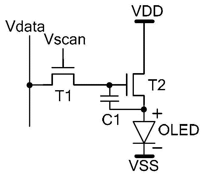
[0049] Embodiments of the present invention provide an array substrate, a display device and a manufacturing method, in which the first electrode plate of a storage capacitor is formed through the second region of the transparent oxide active layer, thereby increasing the aperture ratio of the array substrate.

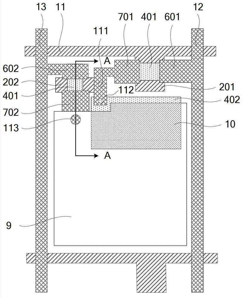
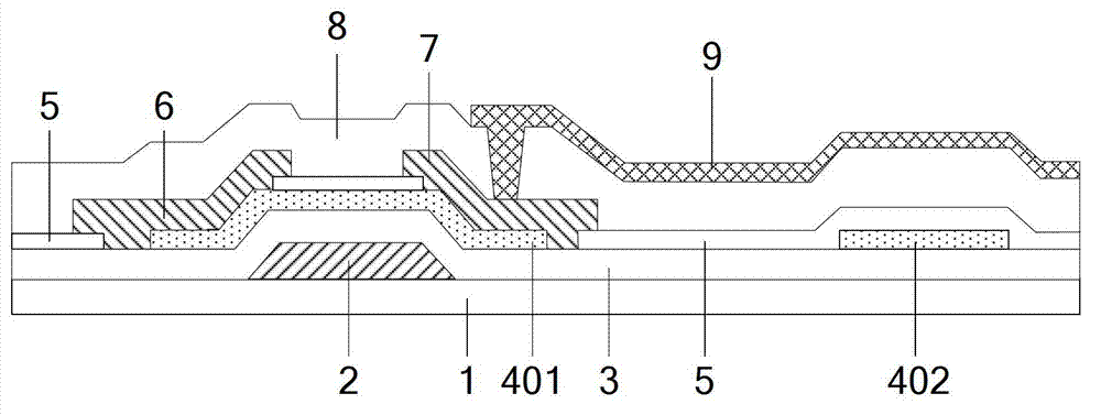
[0050] The following will clearly and completely describe the technical solutions in the embodiments of the present invention with reference to the accompanying drawings in the embodiments of the present invention. Obviously, the described embodiments are only some, not all, embodiments of the present invention. Based on the embodiments of the present invention, all other embodiments obtained by persons of ordinary skill in the art without making creative efforts belong to the protection scope of the present invention. The film thickness and area size and shape of each layer in the drawings do not reflect the true proportion of the AMOLED (Active Matrix OLED, Active Mat...


PUM


Abstract

The embodiment of the invention discloses an array substrate, a display device and a manufacturing method, and relates to the technical field of display devices. A second area of a transparent oxide active layer is used for forming a first electrode plate of a storage capacitor, so that the aperture ratio of the array substrate is increased. The array substrate comprises the oxide active layer and a pixel electrode, wherein the oxide active layer comprises patterns of first and second areas of the oxide active layer; the pixel electrode and the corresponding part of the second area of the oxide active layer form the storage capacitor; the second area of the oxide active layer forms the first electrode plate of the storage capacitor; the pixel electrode opposite to the second area of the oxide active layer forms a second electrode plate of the storage capacitor; and a film layer between the first and second electrode plates form a dielectric substance of the storage capacitor.

Description

technical field [0001] The present invention relates to the technical field of display devices, in particular to an array substrate, a display device and a manufacturing method. Background technique [0002] In recent years, with the continuous advancement and improvement of the level of science and technology, display technology has developed rapidly. Based on its advantages such as high-quality image display, self-illumination, fast response speed, and wide viewing angle, OLED (Organic Light-Emitting Diode, organic light-emitting diode display) occupies a broad market in the display field, and more and more OLED Display devices are well known and widely used in daily life. [0003] However, the inventors have found that at least the following problems exist in the array substrate of the prior art: the storage capacitor in the OLED drive circuit in the prior art is formed by opaque metal electrodes and pixel electrodes, therefore, the opaque metal electrodes directly affec...

Claims


Application Information

Patent Timeline
Patent Type & Authority Applications(China)
IPC IPC(8): H01L27/32H01L21/77
CPCH01L21/443H01L27/1255H01L27/1259H01L29/7869H01L27/1225H10K59/1216H10K59/1213H01L21/02565H01L21/02664H01L21/47635H01L29/24H01L29/66969
Inventor 成军陈江博孔祥永
Owner BOE TECH GRP CO LTD
Why Eureka
Try Eureka