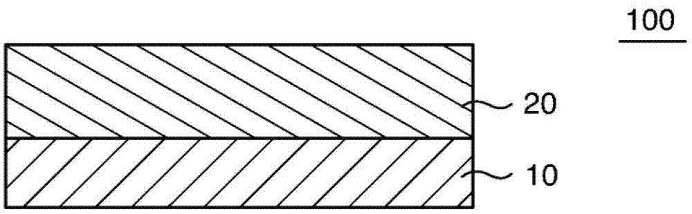
Supercharge Your Innovation With Domain-Expert AI Agents!

Binding tape

An adhesive tape and adhesive layer technology, applied in the direction of adhesives, film/sheet adhesives, electrical components, etc., can solve adhesive residues, damage to semiconductor wafers, insufficient height difference followability, etc. problem, to achieve the effect of fewer steps and excellent followability of height differences

Inactive Publication Date: 2013-08-14
NITTO DENKO CORP
View PDF4 Cites 1 Cited by
  • Summary
  • Abstract
  • Description
  • Claims
  • Application Information

AI Technical Summary

Problems solved by technology

However, the materials that can be used for co-extrusion are thermoplastic resins, and when thermoplastic resins are used, it is difficult to achieve both moderate adhesive force and conformability to the irregularities of the semiconductor wafer pattern (level difference followability)
That is, for an adhesive tape whose adhesive force is adjusted so that it can be easily peeled off, the adhesive becomes too hard and the level difference followability is insufficient, and the purpose of protecting the semiconductor wafer cannot be fully achieved.
On the other hand, the adhesive tape adjusted to exhibit good level difference followability has too strong adhesive force, and there is a problem that the semiconductor wafer is damaged during peeling, and the adhesive remains on the semiconductor wafer.

Method used


Image

  • Binding tape
  • Binding tape
  • Binding tape

Examples


Embodiment 1

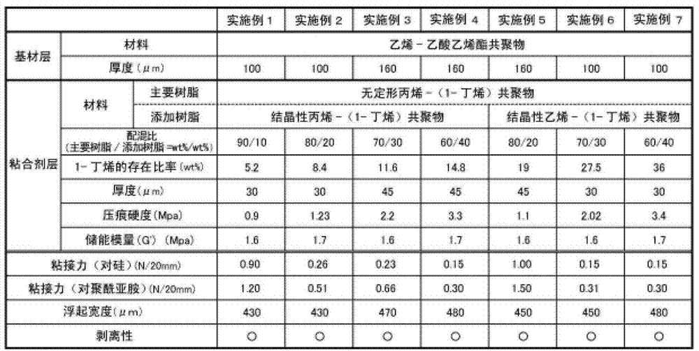
[0076] As an adhesive layer forming material, an amorphous propylene-(1-butene) copolymer (manufactured by Sumitomo Chemical Co., trade name "Tafthren H5002", derived from 1-butene) containing 90 parts by metallocene catalyst polymerization was used. structural unit: 2% by weight), and 10 parts of crystalline propylene-(1-butene) copolymer (manufactured by Mitsui Chemicals, trade name "TAFMER XM7070", structural unit derived from 1-butene: 34% by weight) (total content ratio of structural units derived from 1-butene in the resin composition: 5.2% by weight).

[0077] As the substrate layer forming material, an ethylene-vinyl acetate copolymer (manufactured by DuPont-Mitsui Co., Ltd., trade name "EVAFLEX P1007") was used.

[0078] The above-mentioned adhesive layer forming material and base material layer forming material were charged into respective extruders, and T-die melt coextrusion was carried out (extruder: manufactured by GM Engineering, trade name "GM30-28" / T-die : Cl...

Embodiment 2

[0080]As an adhesive layer forming material, an amorphous propylene-(1-butene) copolymer (manufactured by Sumitomo Chemical Co., trade name "Tafthren H5002", derived from 1-butene) containing 80 parts by metallocene catalyst polymerization was used. structural unit: 2% by weight), and 20 parts of crystalline propylene-(1-butene) copolymer (manufactured by Mitsui Chemicals, trade name "TAFMER XM7070", structural unit derived from 1-butene: 34% by weight) (total content ratio of structural units derived from 1-butene in the resin composition: 8.4% by weight), except that, it was carried out in the same manner as in Example 1 to obtain an adhesive tape.

Embodiment 3

[0082] As an adhesive layer forming material, an amorphous propylene-(1-butene) copolymer (manufactured by Sumitomo Chemical Co., trade name "Tafthren H5002", derived from 1-butene) containing 70 parts by metallocene catalyst polymerization was used. structural unit: 2% by weight), and 30 parts of crystalline propylene-(1-butene) copolymer (manufactured by Mitsui Chemicals, trade name "TAFMER XM7070", structural unit derived from 1-butene: 34% by weight) (total content ratio of structural units derived from 1-butene in the resin composition: 11.6% by weight), the thickness of the adhesive layer is 45 μm, and the thickness of the substrate layer is 160 μm. In addition, with Embodiment 1 was operated similarly to obtain an adhesive tape.


PUM

PropertyMeasurementUnit
storage modulusaaaaaaaaaa
thicknessaaaaaaaaaa
thicknessaaaaaaaaaa

Abstract

The present invention provides a binding tape with excellent balance and pursuit performance between a binding force and a peeling performance and can be manufactured through co-extrusion forming. The binding tape of the invention is provided with a binder layer which is made of a resin composition that comprises amorphous propylene-(1-butylene) copolymer. When the binding tape is adhibited on a bound article with 30 mu m height difference, the binding tape floats at the part next to the lower part of the height difference. The width of the contact part between the binding tape and the bound article is less than 650 mu m. According to measurement through a method of JIS Z0237(2000) with measurement conditions (binding condition of pressing once by a 2kg roller, peeling speed of 300mm / minute and peeling angle of 180 DEG), the binding force of the binding tape to a silicon semiconductor mirror wafer is less than 2.0N / 20mm.

Description

technical field [0001] This invention relates to adhesive tapes. Background technique [0002] Semiconductor wafers made of silicon, gallium, arsenic, etc. are manufactured in a large-diameter state. After the surface is patterned, the back surface is ground. The thickness of the wafer is usually reduced to about 100-600 μm, and then dicing is separated into component pieces. , and then transferred to the installation process. [0003] In the process of grinding the back surface of the semiconductor wafer (back grinding process), an adhesive tape is used to protect the pattern surface of the semiconductor wafer. The adhesive tape is usually peeled off after the back grinding process. The adhesive tape used for this purpose must have an adhesive force that will not peel off in the back grinding process. On the other hand, it is also required that it can be easily peeled off after the back grinding process without damaging the semiconductor crystal. Low adhesion to roundnes...

Claims


Application Information

Patent Timeline
Patent Type & Authority Applications(China)
IPC IPC(8): C09J7/02C09J123/14C09J123/08H01L21/683
Inventor 土生刚志龟井胜利生岛伸祐浅井文辉
Owner NITTO DENKO CORP
Features
  • R&D
  • Intellectual Property
  • Life Sciences
  • Materials
  • Tech Scout
  • Unparalleled Data Quality
  • Higher Quality Content
  • 60% Fewer Hallucinations
Learn More