

PCB correction method and correction device
A technology of PCB board and steel plate, applied in the field of PCB board correction method and correction device, can solve the problems of inconvenient operation and easy scratching of the PCB board, multiple handling of the PCB board, complicated device structure, etc., so as to improve the utilization rate of equipment and simplify the internal Structural structure, the effect of simplifying the process
- Summary
- Abstract
- Description
- Claims
- Application Information
AI Technical Summary
Problems solved by technology
Method used
Image

Examples
Embodiment 1
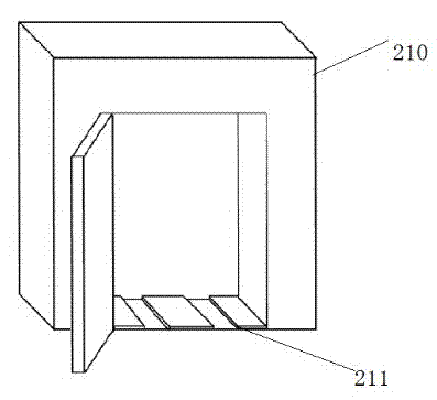
[0033] Such as figure 2 and image 3 A PCB straightening device shown includes an oven 210 and a carrier 220 that can enter and exit the oven. The bottom of the carrier 220 is provided with rollers 221 , and the bottom of the oven 210 is provided with guide rails 211 matching the rollers.
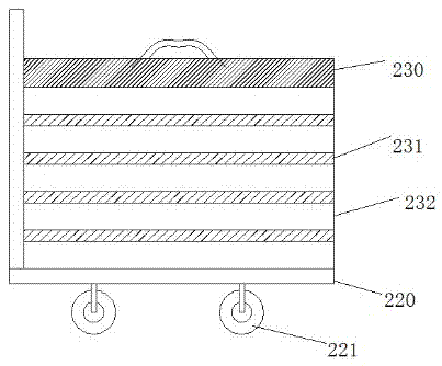
[0034] The above-mentioned carrier 220 is also provided with a pressurizing component. In this embodiment, the above-mentioned pressing assembly includes a pressing steel plate 230 .
[0035] In addition, there is a heat transfer component under the pressure steel plate, including 4 heat transfer steel plates 231 that can be arranged at intervals between the stacked PCB boards. The thickness of the heat transfer steel plate is 1mm, and the surface of the heat transfer steel plate is coated with 0.05mm aluminum thermal conductivity layer.
[0036] The method of using the above device to correct the PCB board is as follows:
[0037] a. The PCB boards to be processed are stacked into 5 P...
PUM
| Property | Measurement | Unit |
|---|---|---|
| Thickness | aaaaa | aaaaa |
Abstract
Description
Claims
Application Information