Flip-chip welding spot defect back view temperature measurement detecting method

A flip-chip and flip-chip welding technology, which is applied in the field of chip solder joint defect detection, can solve the problem that the detection technology cannot meet the actual needs of production, and achieve the effects of a wide range of applicable processes, defect identification rate, and high identification rate.

Inactive Publication Date: 2013-08-21
HARBIN INST OF TECH
View PDF4 Cites 15 Cited by
  • Summary
  • Abstract
  • Description
  • Claims
  • Application Information

AI Technical Summary

Problems solved by technology

[0009] Aiming at the defect that the existing detection technology cannot meet the actual demand of production, the prese

Method used


Image

  • Flip-chip welding spot defect back view temperature measurement detecting method
  • Flip-chip welding spot defect back view temperature measurement detecting method
  • Flip-chip welding spot defect back view temperature measurement detecting method

Examples


Embodiment Construction

[0025] The technical solution of the present invention will be further described below in conjunction with the accompanying drawings, but it is not limited to this. Any modification or equivalent replacement of the technical solution of the present invention without departing from the spirit and scope of the technical solution of the present invention should be covered by the technical solution of the present invention. in the scope of protection.

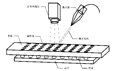
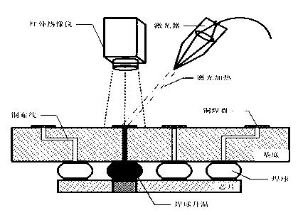
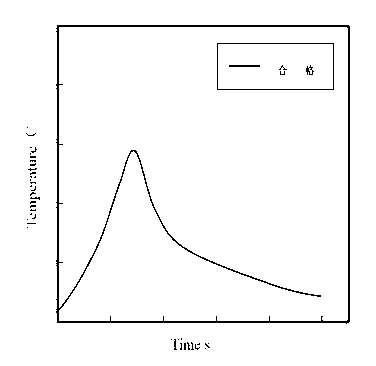
[0026] Such as figure 1 As shown, a thermal imager and an infrared laser are respectively arranged on the substrate side of the flip chip, and the diameter of the laser beam is slightly smaller than that of the bonding pad. Aim the infrared laser beam at the pad to be tested on the flip chip substrate, adjust the power and pulse width parameters, and apply thermal excitation to it, that is, input a fixed amount of heat to the pad, during which the temperature of the pad rises rapidly , the heat is conducted to the solder balls an...


PUM


Abstract

The invention discloses a flip-chip welding spot defect back view temperature measurement detecting method, and relates to a detecting method of chip welding spot defects. In order to overcome the defect that an existing detecting technology cannot satisfy actual production demands, flip-chip welding spot defects are detected according to the method that a thermal imager and an infrared laser are arranged on one side of a base of a flip-chip respectively, the infrared laser device is flush with a flip-chip base welding disk to be detected, power and pulse width parameters are adjusted, thermal excitation is conducted on the welding disk, the thermal imager detects the temperature rising process of the base welding disk to be detected in real time, and at the same time, a thermo-gram of a temperature rising highest point is observed and shot. Therefore, the welding spot defects are judged according to a temperature rise curve and the thermo-gram. A spot-by-spot detecting method is adopted in the flip-chip welding spot inveracious welding detecting method, and therefore the flip-chip welding spot inveracious welding detecting method has the advantages of being free of abrasion, high in defect identification rate, and visual and simple in judging. In addition, technological range of application is wide, the method is also applicable to defect detecting during chip side ball embedding and defect detecting during base side ball embedding in three-dimensional assembling.

Description

technical field [0001] The invention relates to a detection method for chip solder joint defects, in particular to a detection method for flip-chip solder joint defects. Background technique [0002] With the development of electronic packaging technology in the direction of high density, high performance and miniaturization, BGA (Ball Grid Array) packaging has become the mainstream of contemporary electronic packaging. Ceramic ball grid array CBGA (CeramicBall Grid Array), as a packaging form of BGA, is widely used in military, aviation and aerospace electronic equipment manufacturing fields due to its high I / O density, high reliability and good electrical and thermal performance . CCGA (Ceramic Column Grid Array) is an improvement based on CBGA. It replaces the ball array with a column array, which relieves the shear stress between the ceramic substrate and the PCB caused by thermal mismatch, and improves thermal cycle reliability. [0003] The miniaturization of microel...

Claims


Application Information

Patent Timeline
IPC IPC(8): H01L21/66G01N25/72
Inventor 孔令超田艳红王春青杭春进刘宝磊
Owner HARBIN INST OF TECH
Why Eureka
Try Eureka