Distress signal receiving module and decoding method thereof

A technology of receiving module and distress signal, applied in the field of signal receiving module and its decoding

Inactive Publication Date: 2013-08-21
BEILUN SCI & ART EXPERIMENT CENT INST OF AUTOMATION CHINESES ACADEMY OF SCI
5 Cites 0 Cited by

AI-Extracted Technical Summary

Problems solved by technology

[0004] The purpose of the present invention is to solve the problem that the prior art sends and receives signals, and when the signals are encoded and decoded, it cannot achieve better output in a harsher working environment, and provides a kind of performance and qualit...

Abstract

The invention relates to a distress signal receiving module and a decoding method thereof. The distress signal receiving module and the decoding method thereof can solve the problems that the prior art is influenced greatly by severe environments, and is poor in quality and performance. According to the technical scheme, the distress signal receiving module comprises a stabilizing power supply circuit for supplying power, a receiving antenna, a receiving module controller, a bus interchanger, a protector circuit, a filter circuit, a mixed frequency amplifying circuit, a modem circuit, a receiving module first memorizer, a USB integrated circuit and a receiving module second memorizer. The receiving module controller is connected with a processor module through the bus interchanger. The filter circuit is connected with the input end of the filter circuit through the protector circuit. The output end of the filter circuit is connected with the input end of the mixed frequency amplifying circuit. The control end of the mixed frequency amplifying circuit is connected with the receiving module controller. The output end of the mixed frequency amplifying circuit is connected with the input end of the modem circuit. The output end of the modem circuit is connected with the receiving module controller. The distress signal receiving module is good in quality and performance.

Application Domain

AlarmsTransmission

Technology Topic

Integrated circuitEnvironment effect +7

Image

  • Distress signal receiving module and decoding method thereof
  • Distress signal receiving module and decoding method thereof
  • Distress signal receiving module and decoding method thereof

Examples

  • Experimental program(1)
  • Effect test(1)

Example Embodiment

[0048] Examples:
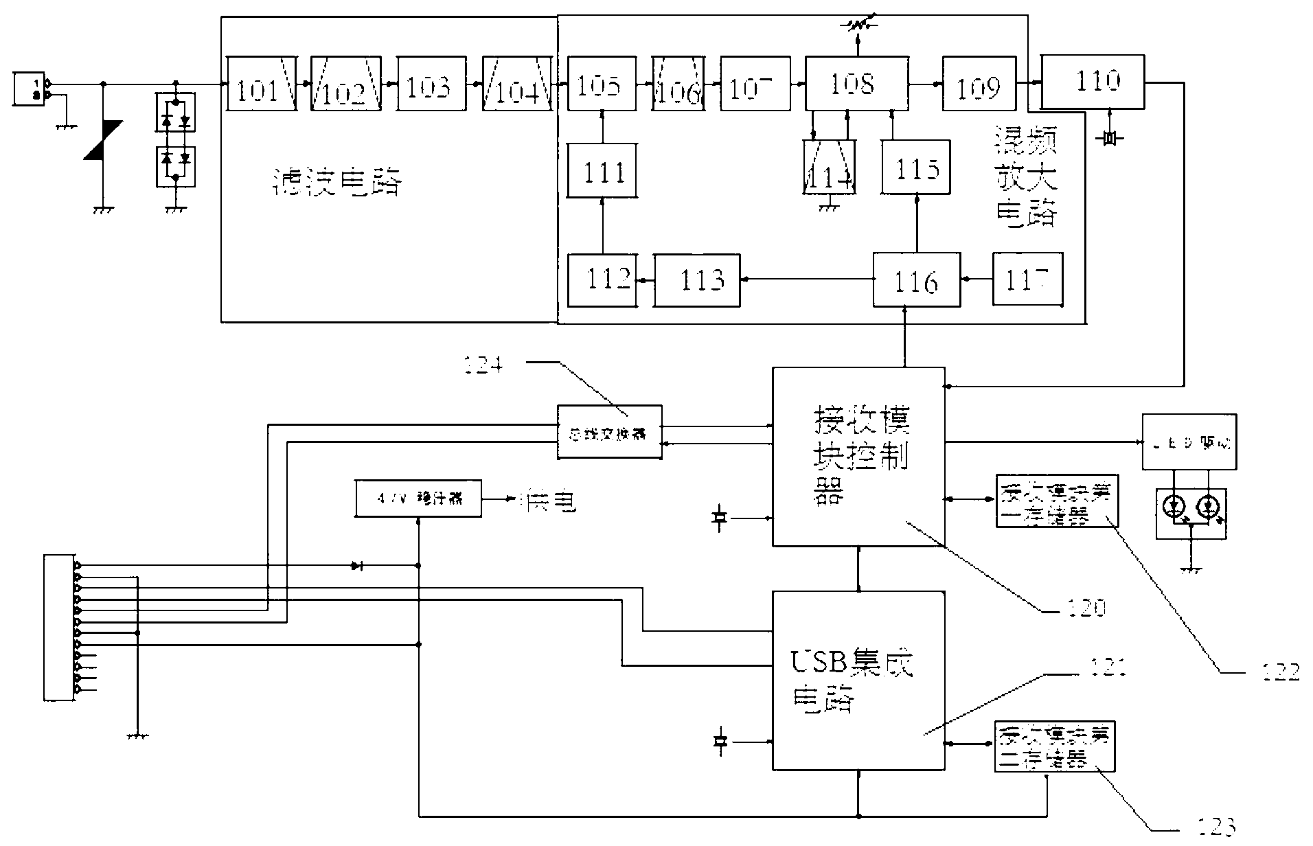
[0049] A distress signal receiving module (see attached figure 1 ) Installed on the embedded search and rescue chartplotter, including a regulated power supply circuit for power supply, a receiving antenna, a receiving module controller 120 composed of a single-chip circuit, a bus switch 124, a protector circuit, a filter circuit, and a mixer amplifier circuit , The modem circuit, the first memory 122 of the receiving module, the USB integrated circuit 121 and the second memory 123 of the receiving module, the receiving module controller is connected to the processor module through the bus switch, and the filter circuit is connected through the protector The circuit is connected to the input end of the filter circuit, the output end of the filter circuit is connected to the input end of the mixer amplifier circuit, the control end of the mixer amplifier circuit is connected to the receiving module controller, and the mixer The output terminal of the amplifying circuit is connected with the input terminal of the modem circuit, the output terminal of the modem circuit 110 is connected with the receiving module controller, and the receiving module controller is also electrically connected with the first memory of the receiving module and the USB integrated circuit, The second memory of the receiving module is electrically connected with the USB integrated circuit. The filter circuit includes a receiving module low-pass filter 101, a first band-pass filter 102, a radio frequency amplifier 103, and a second band-pass filter 104 connected in series in sequence. The input end of the receiving module low-pass filter is connected to the protection The output terminal of the filter circuit is connected, and the output terminal of the second band-pass filter is connected with the input terminal of the mixing amplifier circuit. The mixing amplifier circuit includes a reference oscillator circuit 114, a first mixer 105, a monolithic crystal filter 106, an intermediate frequency amplifier 107, an intermediate frequency integrated circuit 108, an audio amplifier 109, a first amplifier 111, a second amplifier 115, The buffer amplifier 112, the receiving voltage-controlled oscillator 113, the phase-locked loop 116 and the temperature-compensated crystal oscillator 117, the first input end of the first mixer is connected to the output end of the filter circuit, and the first mixer The second input terminal is connected to the output terminal of the first amplifier, the receiving voltage controlled oscillator is connected to the input terminal of the first amplifier through the buffer amplifier, and the input terminal of the receiving voltage controlled oscillator is connected to the first output terminal of the phase-locked loop. The input end of the phase-locked loop is electrically connected to the receiving module controller, the crystal oscillator end of the phase-locked loop is connected to the temperature-compensated crystal oscillator, and the second output end of the phase-locked loop is controlled by the intermediate frequency integrated circuit through the second amplifier. The output terminal of the first mixer is electrically connected to the input terminal of the intermediate frequency integrated circuit through the monolithic crystal filter, the reference input terminal of the intermediate frequency integrated circuit is connected to the reference oscillator circuit, and the output terminal of the intermediate frequency integrated circuit is connected through the audio frequency The amplifier is electrically connected with the modulation and demodulation circuit.
[0050] The embedded search and rescue chartplotter (see attached figure 2 ), including a power supply system and a working system, the working system is electrically connected to the power supply system, characterized in that: the working system includes a processor module 10 composed of a single-chip circuit, and a control composed of a control button 1 Button module, interface module 2, display module 3, speaker module 4, positioning module 5, data memory 6 and program memory 7, all the control buttons, interface module, display module, speaker module, positioning module, data memory and program The memories are electrically connected with the processor module. The power supply system includes a power management module 20, a battery 21, an auxiliary power system 22, a DC charging module 23, and a USB charging module 24. The battery, auxiliary power system, DC charging module, and USB charging module are all compatible with the The power management module is electrically connected. The embedded search and rescue chartplotter also includes a distress signal receiving module 8 and a distress signal transmitting module 9. Both the distress signal receiving module and the distress signal transmitting module are electrically connected to the processor module.
[0051] The distress signal transmitter module (see attached image 3 ) Including a voltage stabilizing circuit 217 for power supply, a transmitting antenna, a connection interface, a frequency adjustment circuit, a radio frequency amplifier circuit, a feedback control circuit and a low-pass filter circuit. The input end of the frequency adjustment circuit is connected to the processor module through a connection interface , The output end of the frequency adjustment circuit is connected to the input end of the radio frequency amplifying circuit, the output end of the radio frequency amplifying circuit is connected to the transmitting antenna through the low-pass filter circuit, and the input end of the feedback control circuit is connected to the processing The feedback input terminal of the feedback control circuit is connected with the low-pass filter circuit, and the control output terminal of the feedback control circuit is connected with the control terminal of the radio frequency amplifier circuit. The low-pass filter circuit includes a first low-pass filter 204, a second low-pass filter 203, a third low-pass filter 202, and a fourth low-pass filter 201 serially connected in series. The input terminal is connected to the output terminal of the radio frequency amplifying circuit, the output terminal of the fourth low-pass filter is connected to the transmitting antenna, and the output terminal of the second low-pass filter is connected to the feedback control circuit as a feedback output terminal; the feedback The control circuit includes an automatic control phase amplifier 215, a transmission control switch 216, and a power adjustment resistor. The automatic control phase amplifier is connected to the voltage stabilizing circuit through the power adjustment resistor. The input end of the automatic control phase amplifier is connected with the transmission control switch. Interface connection, the feedback output end of the automatic control phase amplifier is connected to the feedback input end of the radio frequency amplifier circuit; the frequency adjustment circuit includes a frequency fine adjustment module 214, a frequency adjustment resistor, a deviation adjustment resistor, a crystal 213, an oscillator 212, Send the buffer amplifier 211 and the high-pass filter 210, the output terminal of the voltage stabilizing circuit is connected to the first input terminal of the frequency fine-tuning module through a frequency adjusting resistor, and the modulation signal output terminal of the connection interface is connected to the frequency fine-tuning module through a deviation adjusting resistor. The second input terminal is connected, the output terminal of the frequency fine-tuning module is connected to the high-pass filter through the crystal oscillator, the oscillator and the transmitting buffer amplifier in sequence, and the output terminal connected to the high-pass filter is connected to the input terminal of the radio frequency amplifier circuit; the radio frequency The amplifying circuit includes a first radio frequency amplifier 209, a second radio frequency amplifier 208, a third radio frequency amplifier 207, a fourth radio frequency amplifier 206, and a fifth radio frequency amplifier 205 connected in series in sequence, the input end of the first radio frequency amplifier and the frequency adjustment circuit. The output end is connected, the output end of the fifth radio frequency amplifier is connected to the input end of the low-pass filter circuit, the fourth radio frequency amplifier and the fifth radio frequency amplifier are radio frequency amplifiers with feedback interfaces, and the fourth radio frequency amplifier and The feedback interfaces of the fifth radio frequency amplifier are all electrically connected to the feedback control circuit. The interface module includes a master-slave USB interface, an RS232 interface, and a TF card interface. The master-slave USB interface, RS232 interface, and TF card interface are all electrically connected to the processor module. The display module includes LCD and touch display. The LCD module and the touch display module are both connected to the processor module, and the positioning module is a GPS module or a Beidou module.

PUM

no PUM

Description & Claims & Application Information

We can also present the details of the Description, Claims and Application information to help users get a comprehensive understanding of the technical details of the patent, such as background art, summary of invention, brief description of drawings, description of embodiments, and other original content. On the other hand, users can also determine the specific scope of protection of the technology through the list of claims; as well as understand the changes in the life cycle of the technology with the presentation of the patent timeline. Login to view more.
Why Eureka
Try Eureka