
Printed circuit board and differential signal line wiring method based on printed circuit board

A technology of differential signal lines and printed circuit boards, applied in the direction of printed circuit components, etc., can solve problems such as prolonging product development cycle, affecting signal transmission quality, increasing wiring complexity, etc., to improve transmission quality, reduce electromagnetic interference, The effect of simple wiring

Active Publication Date: 2016-01-20
HISENSE BROADBAND MULTIMEDIA TECH
View PDF7 Cites 0 Cited by
  • Summary
  • Abstract
  • Description
  • Claims
  • Application Information

AI Technical Summary

Problems solved by technology

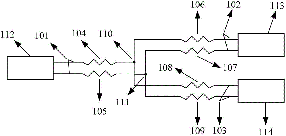
For example, in the existing PCB, the circuit module A and the circuit module B are connected through a differential signal line pair. If the function of the PCB needs to be expanded so that the circuit module A can be connected to the circuit module C corresponding to the extended function through a differential signal line pair, then It is necessary to re-wire the differential signal line pairs between circuit module A and circuit module B, and between circuit module A and circuit module C on the same layer of the PCB to which circuit module A and circuit module B belong, making the wiring complicated The reliability also increases accordingly; furthermore, when multiple pairs of differential signals are transmitted in the same layer, there is mutual electromagnetic interference between the differential signal line pairs, which affects the transmission quality of the signal and prolongs the product development cycle

Method used


Image

  • Printed circuit board and differential signal line wiring method based on printed circuit board
  • Printed circuit board and differential signal line wiring method based on printed circuit board

Examples


Embodiment Construction

[0028] In order to make the object, technical solution and advantages of the present invention clearer, the present invention will be described in further detail below with reference to the accompanying drawings and preferred embodiments.

[0029] The invention provides a wiring method for a printed circuit board and its differential signal lines. In the case that the circuit module required for the extended function is shared with any circuit module or multiple circuit modules in the existing PCB, the circuit module corresponding to the extended function is arranged on another layer of the PCB, and via holes are set on the PCB , the differential signal line pair wired by the circuit module on the other layer is connected to the shared circuit module through vias, so as not to affect the wiring method of the PCB layer where the shared module is located; at the same time, the wiring method of the other layer of the PCB is relatively simple, and the layer and The differential si...


PUM


Abstract

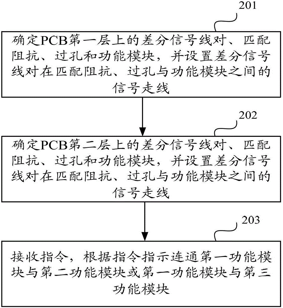
The invention discloses a printed circuit board (PCB) and a differential signal line wiring method based on the PCB. The differential signal line wiring method based on the PCB comprises the steps that signal wiring of a differential signal line on a first layer of the PCB among matching impedance, a via hole and a functional module is laid; signal wiring of a differential signal line on a second layer of the PCB among matching impedance, a via hole and a functional module is laid; commands are received, and according to command indication, a first functional module is communicated with a second functional module or the first functional module is communicated with a third functional module. According to the PCB and the differential signal line wiring method based on the PCB, wiring complexity in function expansion of the PCB can be reduced.

Description

technical field [0001] The present invention relates to the technical field of printed circuit board (PCB, Printed Circuit Board), in particular to a PCB and a method for wiring differential signal lines based on the PCB. Background technique [0002] In PCB, when it is necessary to perform signal transmission between two circuit modules, the signal to be transmitted is usually subjected to differential processing to obtain a differential signal, which is arranged as a pair of differential signal lines close to parallel. In this way, in the case of impedance matching, due to the mutual coupling of the differential signals in the two parallel traces, external common-mode noise can be offset and electromagnetic interference can be effectively suppressed. [0003] In the PCB, the distance between the differential signal line pairs of parallel traces is kept constant at any position along the trace direction. In the prior art, the two circuit modules and the differential signal...

Claims


Application Information

Patent Timeline
Patent Type & Authority Patents(China)
IPC IPC(8): H05K1/02
Inventor 高均波
Owner HISENSE BROADBAND MULTIMEDIA TECH
Learn More