
Apparatus and method for directional solidification of silicon

A technology of directional solidification and molten silicon, which is applied in chemical instruments and methods, silicon compounds, inorganic chemistry, etc., can solve the problems of high cost, limited economic efficiency of silicon purification devices and methods, and high production cost of large crucibles, so as to reduce waste Effect

Active Publication Date: 2016-11-30
SILICOR MATERIALS INC
View PDF10 Cites 0 Cited by
  • Summary
  • Abstract
  • Description
  • Claims
  • Application Information

AI Technical Summary

Problems solved by technology

Although made from cheaper materials, large crucibles made of fused silica or other refractory materials are still expensive to produce and are usually only used once
The combination of high cost and limited lifetime of crucibles limits the economic efficiency of silicon purification apparatus and methods

Method used


Image

  • Apparatus and method for directional solidification of silicon
  • Apparatus and method for directional solidification of silicon
  • Apparatus and method for directional solidification of silicon

Examples


preparation example Construction

[0024] In the preparative methods described herein, unless a chronological or operational sequence is explicitly indicated, the steps may be performed in any order without departing from the principles of the invention. When it is described in a claim that a step is performed first followed by several other steps, it is to be understood that it means that the first step is performed before all other steps, but that the other steps may be performed in any suitable order unless the other steps are performed The sequence is described further in . For example, a claim element that describes "step A, step B, step C, step D, and step E" should be understood to mean that step A is performed first, and step E is performed last, and that steps B, C, and D can be performed between steps A and E can be performed in any order that still falls within the literal scope of the claimed method. A given step or subset of steps may also be repeated.

[0025]Furthermore, certain steps may be pe...

Embodiment approach 1

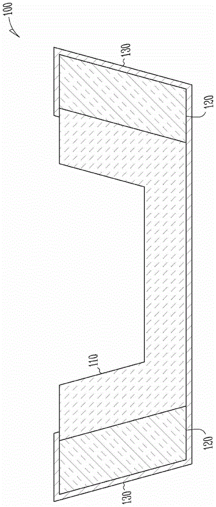
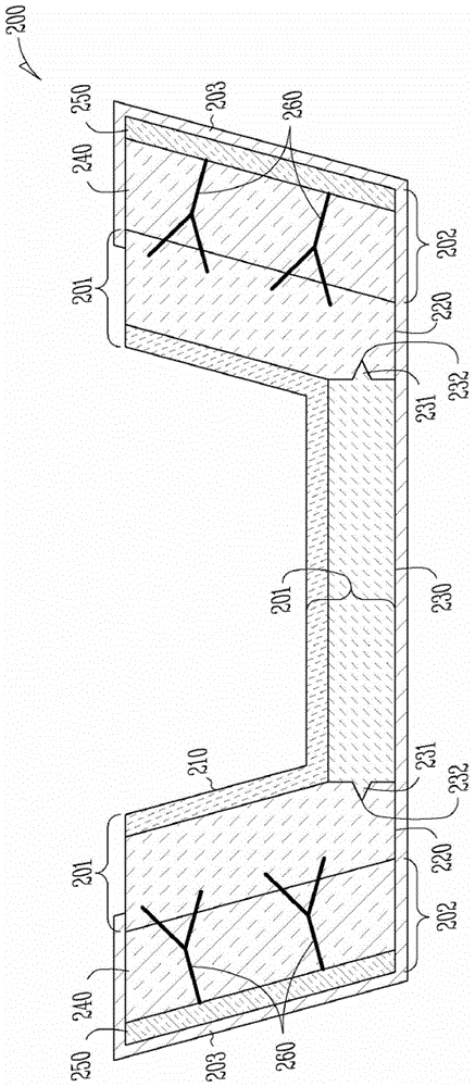
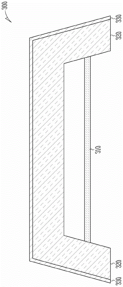
[0106] Embodiment 1. Apparatus for directional solidification of silicon comprising:

[0107] a directionally solidified mold comprising at least one refractory material;

[0108] casing; and

[0109] An insulating layer at least partially disposed between the directional curing mold and the shell.

Embodiment approach 2

[0110] Embodiment 2. The device of embodiment 1, wherein the directional curing mold, housing, and thermal barrier are configured for more than two directional curing of silicon.


PUM

PropertyMeasurementUnit
boiling pointaaaaaaaaaa

Abstract

The present invention relates to apparatus and methods for purifying silicon using directional solidification. The device can be used for directional curing of silicon more than once without failure. The apparatus and method of the present invention can be used to manufacture silicon crystals for use in solar cells.

Description

[0001] claim priority [0002] This application claims the benefit of priority to US Patent Application Serial No. 12 / 947,936, filed November 17, 2010, which is hereby incorporated by reference in its entirety. Background technique [0003] Solar cells can be a viable energy source by harnessing their ability to convert sunlight into electricity. Silicon is the semiconductor material used in the manufacture of solar cells, however, a limitation of the use of silicon relates to the cost of purifying it to solar grade (SG). [0004] Several techniques are known for the manufacture of silicon crystals for solar cells. The operating principle of most of these techniques is that when silicon solidifies from a molten solution, undesired impurities tend to remain in the molten solution. For example, floating zone technology can be used to create single crystal ingots and use a moving liquid zone in the solid material to move impurities to the edge of the material. In another examp...

Claims


Application Information

Patent Timeline
Patent Type & Authority Patents(China)
IPC IPC(8): C30B28/06C01B33/037C30B29/06H01L31/18
Inventor S·尼科尔D·史密斯
Owner SILICOR MATERIALS INC
Learn More