Multi-working-voltage input-output pin unit circuit

A technology of working voltage, input and output, applied in the direction of logic circuit coupling/interface, logic circuit connection/interface arrangement using field effect transistors, etc., can solve problems such as excessive source-drain voltage, failure, excessive gate voltage, etc., to achieve Effect of reducing power consumption and improving reliability

Active Publication Date: 2014-12-10
PEKING UNIV
View PDF6 Cites 0 Cited by
  • Summary
  • Abstract
  • Description
  • Claims
  • Application Information

AI Technical Summary

Problems solved by technology

[0006] like figure 1 The problem of the prior art shown is: when the input and output pin units work at different voltages, for example, the working voltage of the Dout terminal is 0 to 1.2V when outputting, and the working voltage of the PAD terminal is 0 to 2.5V when inputting
In a typical situation, OE is low level, and PAD inputs high level 2.5V. At this time, the problems caused are: the output driver stage PMOS is turned on, and at the same time, the parasitic PN node of the output driver stage PMOS is forward-conducted. Both cause leakage from the PAD terminal to the VDD terminal, which affects the normal operation of the circuit. In addition, the source-drain voltage of the output driver stage NMOS is too large, and the gate voltage of the input driver stage inverter is too large, which may cause breakdown and failure of the transistor.

Method used


Image

  • Multi-working-voltage input-output pin unit circuit
  • Multi-working-voltage input-output pin unit circuit
  • Multi-working-voltage input-output pin unit circuit

Examples


Embodiment Construction

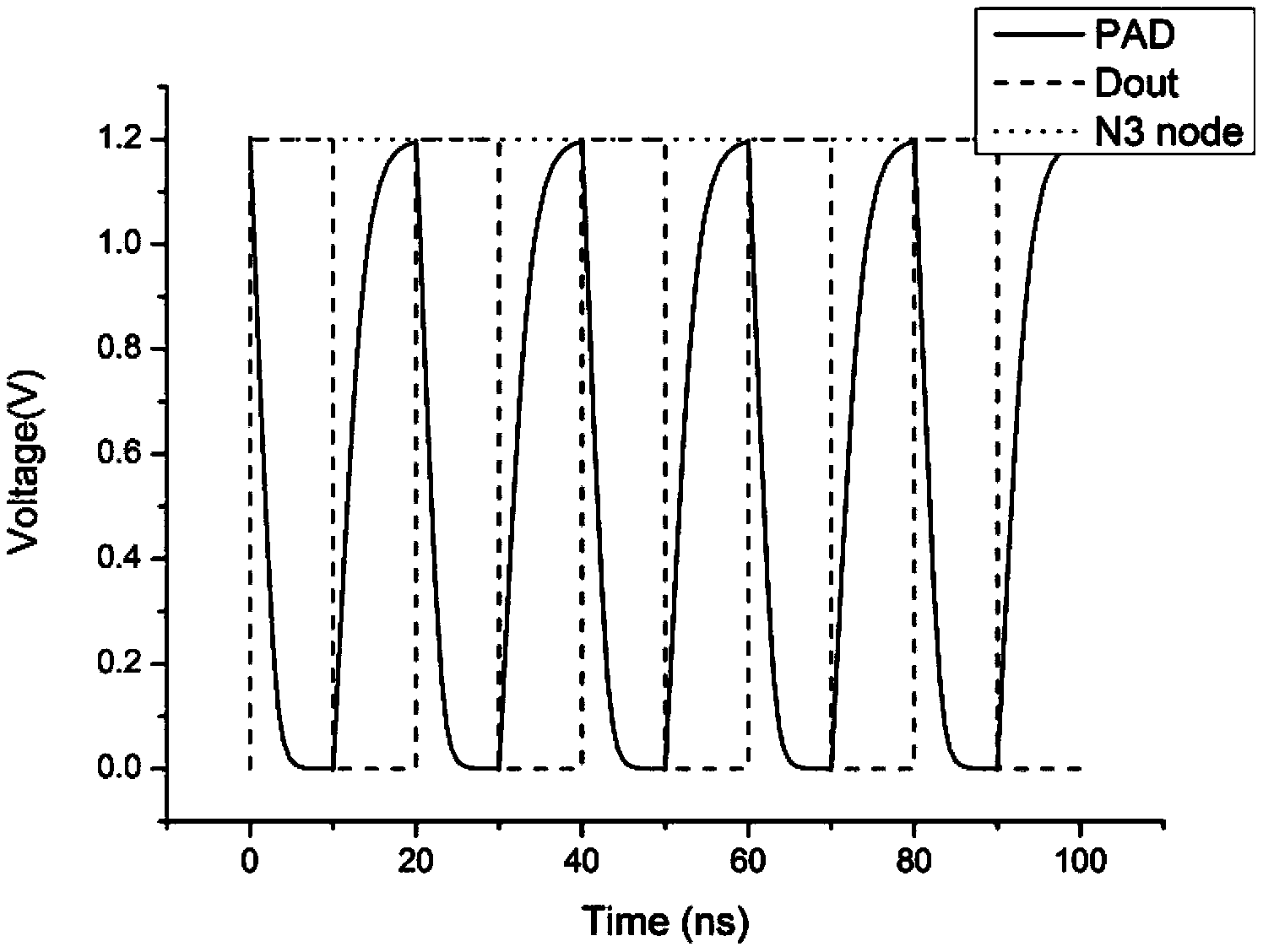
[0044] The specific implementation manners of the present invention will be further described in detail below in conjunction with the accompanying drawings and embodiments. The following examples are used to illustrate the present invention, but are not intended to limit the scope of the present invention.

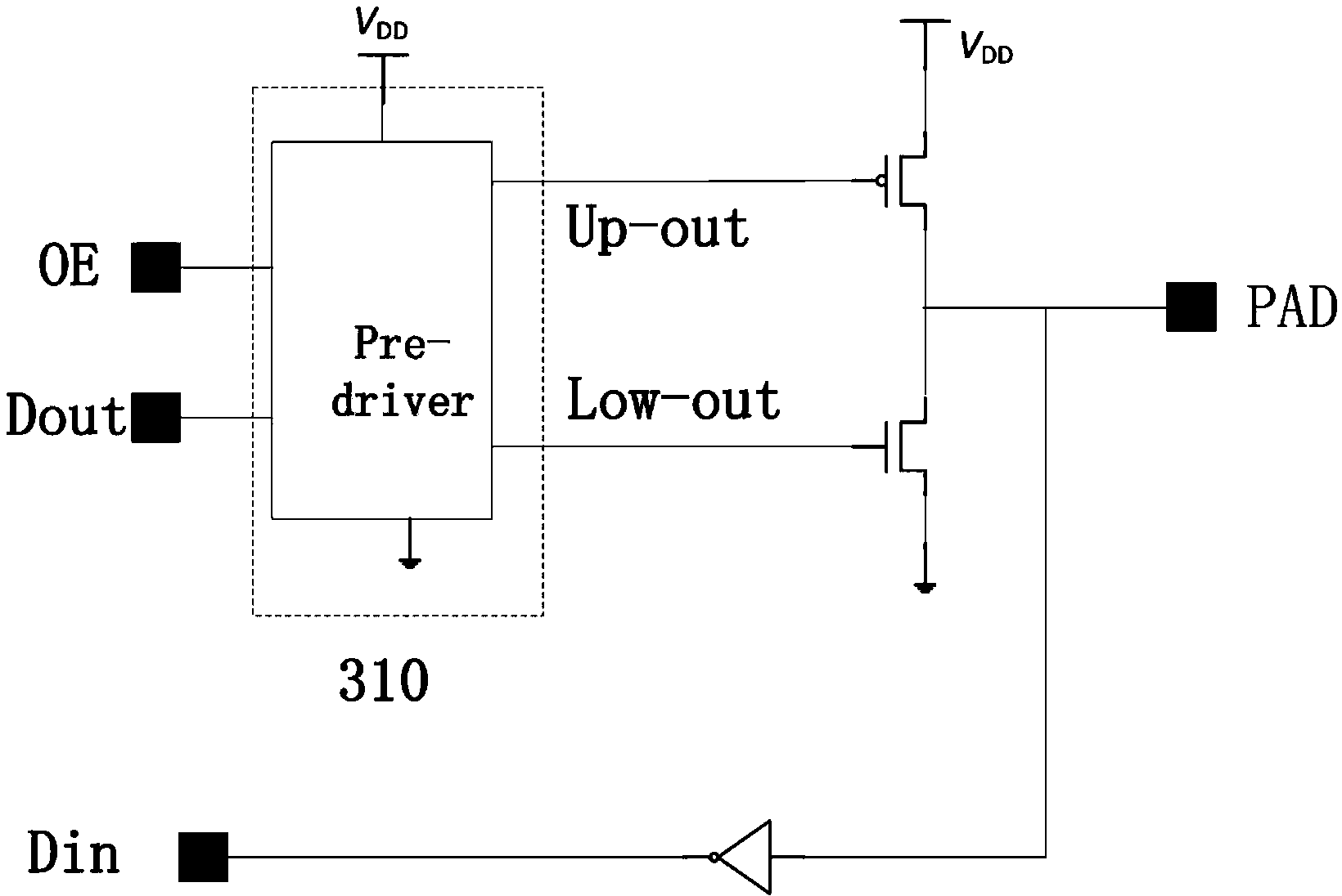
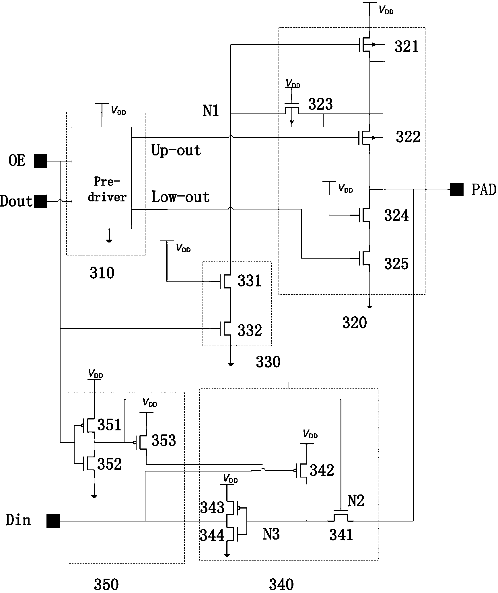
[0045] Such as figure 2 As shown, the multi-operating voltage input and output pin unit circuit proposed by the present invention includes a power supply pin VDD, a ground pin VSS, a pre-driver circuit 310, an output stage drive circuit 320, an output stage protection circuit 330, an input stage The drive circuit 340 and the input stage protection circuit 350; wherein:

[0046] The power supply pin VDD is used to connect to a power supply to provide a power supply voltage;

[0047] The ground pin VSS is used to provide low level;

[0048] A pre-driver circuit 310, which is connected between the power supply pin and the ground pin, is used to convert the enable signal O...


PUM


Abstract

The invention relates to an input-output pin of an integrated circuit and particularly relates to a low-energy-consumption multi-working-voltage input-output pin unit circuit. The circuit comprises a power supply pin, a grounding pin, a pre-positioned driving circuit, an output-grade driving circuit and an input-grade driving circuit, wherein the pre-positioned driving circuit is connected between the power supply pin and the grounding pin and is used for converting an enable signal OE and a signal Dout to be output into a subsequent output; an input end of the output-grade driving circuit is connected with an output end of the pre-positioned driving circuit and the output-grade driving circuit is used for driving a PAD according to the output of the pre-positioned driving circuit; and an input end of the input-grade driving circuit is connected with the PAD and the input-grade driving circuit is used for driving a Din according a PAD signal. According to the multi-working-voltage input-output pin unit circuit disclosed by the invention, a transistor can be effectively protected and the reliability of the circuit is improved. Meanwhile, when the unit is used as the output, the input-grade driving circuit switched off, so that the power consumption is effectively reduced.

Description

technical field [0001] The invention relates to input and output pins of integrated circuits, in particular to an input and output pin unit circuit with low power consumption and multiple working voltages. Background technique [0002] The input and output unit circuit is a commonly used unit inside the integrated circuit. Generally, the input and output unit has the same operating voltage. However, with the increase of device integration, in the face of problems such as speed and power consumption, the operating voltage of the internal circuit is required to continue to drop. , therefore, the input-output unit circuit requires different internal and external operating voltages, for example, in a typical case of a CMOS process, the input voltage is between 0V and 2.5V, and the output voltage is between 0V and 1.2V. [0003] figure 1 Shown is a prior art input and output pin unit circuit, and its working principle is as follows: [0004] When OE (Output Enable, enable signa...

Claims


Application Information

Patent Timeline
Patent Type & Authority Patents(China)
IPC IPC(8): H03K19/0185
Inventor 王源刘琦陆光易曹健贾嵩张兴
Owner PEKING UNIV
Why Eureka
Try Eureka