Monocrystalline silicon automatic bonding method

An automatic bonding, single crystal silicon technology, applied in chemical instruments and methods, crystal growth, post-processing details, etc., can solve the problems of unfavorable large-scale production of silicon wafers, low production efficiency of silicon wafers, and high production costs

Inactive Publication Date: 2013-09-04
SIP GOLDWAY TECH
View PDF3 Cites 0 Cited by
  • Summary
  • Abstract
  • Description
  • Claims
  • Application Information

AI Technical Summary

Problems solved by technology

This makes the production efficiency of silicon wafers relatively low, and the producti

Method used


Image

  • Monocrystalline silicon automatic bonding method
  • Monocrystalline silicon automatic bonding method

Examples


Embodiment Construction

[0016] In order to make the object, technical solution and advantages of the present invention clearer, the present invention will be described in detail below in conjunction with the accompanying drawings and specific embodiments.

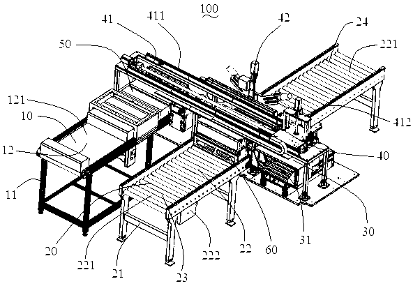
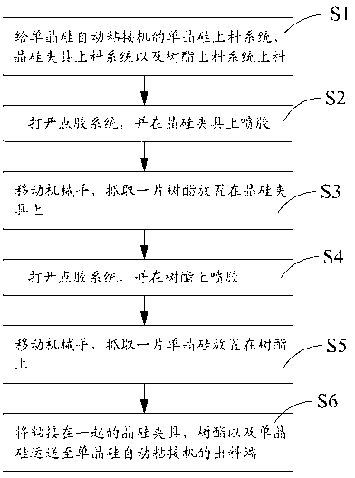
[0017] see figure 1 As shown, the single crystal silicon automatic bonding machine 100 of the present invention is used to realize the automatic bonding of crystal silicon fixtures, resin and single crystal silicon. The single crystal silicon automatic bonding machine 100 includes a single crystal silicon feeding system 10, a crystal silicon fixture feeding system 20, a resin feeding system 30, and a single crystal silicon feeding system 10, a crystal silicon fixture feeding system An operating system 40 that cooperates with the system 20 and the resin feeding system 30 .

[0018] see figure 1 As shown, the single crystal silicon feeding system 10 includes a single crystal silicon feeding rack 11 and a first conveying device 12 installed on the ...


PUM


Abstract

A monocrystalline silicon automatic bonding method is disclosed by the invention, and comprises the following steps: S1. feeding for a monocrystalline silicon feeding system, a crystal silicon clamp feeding system and a resin feeding system of a monocrystalline silicon automatic bonding machine; S2. opening a dispensing system and spraying a binder on the crystal silicon clamp; S3. moving a machinery hand to grab a sheet of resin and place on the crystal silicon clamp; S4. opening the dispensing system and spraying the binder on the resin; S5. moving the machinery hand to grab a sheet of monocrystalline silicon on the resine; S6. deliverying the crystal silicon clamp, the resin and monocrystalline silicon which are bonded together to a discharge end of the monocrystalline silicon automatic bonding machine. Compared with the prior art, the monocrystalline silicon automatic bonding method of the invention can help to achieve an automatic bonding of the crystal silicon clamp, the resin and the monocrystalline silicon.

Description

technical field [0001] The invention relates to a single crystal silicon automatic bonding method. Background technique [0002] When manufacturing silicon wafers, it is necessary to sequentially bond the silicon crystal fixtures, resin, and single crystal silicon used to fix the single crystal silicon with glue. At present, in China, the bonding of the crystal silicon fixture, resin and single crystal silicon is done manually. This makes the production efficiency of the silicon wafer relatively low and the production cost high, which is not conducive to realizing the large-scale production of the silicon wafer. [0003] In view of the above problems, it is necessary to provide a single crystal silicon automatic bonding method to solve the above problems. Contents of the invention [0004] Aiming at the deficiencies of the prior art, the technical problem to be solved by the present invention is to provide an automatic bonding method for single crystal silicon, which can...

Claims


Application Information

Patent Timeline
IPC IPC(8): C30B33/06
Inventor 李佳
Owner SIP GOLDWAY TECH
Why Eureka
Try Eureka