Turnover storing box for storing thin wafer

A technology of wafers and storage boxes, applied in the manufacture of conveyor objects, electrical components, semiconductor/solid-state devices, etc., can solve the problems of collision, unsafe petri dishes, and excessive storage space

Active Publication Date: 2013-09-04
THE 13TH RES INST OF CHINA ELECTRONICS TECH GRP CORP
View PDF7 Cites 4 Cited by
  • Summary
  • Abstract
  • Description
  • Claims
  • Application Information

AI Technical Summary

Problems solved by technology

If it is stored in a cassette, because it is mainly designed to avoid scratches on the surface of a single wafer, it is only suitable for storing relatively thick wafers. The thickness of the wafer after thinning is obviously thinner. are more prone to significant warping and are more likely to shatter if squeezed
If it is stored in a petri dish, if the diameter of the wafer is equal to the inner diameter of the petri dish, it will be difficult to take and place the thinned wafer, and a little carelessness will cause the chip to break; if the diameter does not match, the thinned wafer will The wafer will slide freely in the petri dish, it may collide with the side wall of the petri dish, and it is easy to cause breakage; at the same time, because the petri dish is generally relatively high, it is not conducive to putting in and taking out the thinned wafer , the stacking of multiple petri dishes is neither safe nor will cause too much storage space
Even if the thinned wafer is not scrapped after being broken, it will double the follow-up workload and cause a decrease in the total yield and an increase in cost

Method used


Image

  • Turnover storing box for storing thin wafer
  • Turnover storing box for storing thin wafer
  • Turnover storing box for storing thin wafer

Examples


Embodiment Construction

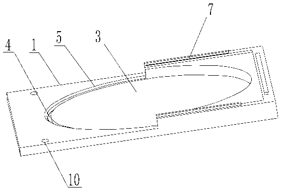
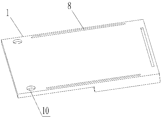
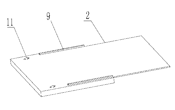
[0020] Such as Figure 1-4 As shown, a turnover storage box for storing thin wafers includes a box body and a box cover. The box body is provided with a cabin platform, the cabin platform is a smooth circular platform, the diameter of the platform is greater than the diameter of the thin wafer; the box body is divided into two parts, high and low, along the partial arc of the cabin platform periphery, and the The lower part of the body is provided with a pick-and-place opening, which is an arc-shaped groove arranged on the outside of the cabin platform. The cover is also divided into high and low parts, the low part of the box cover matches the high part of the box body, and the high part of the box cover matches the low part of the box body.

[0021] Such as Figure 1-2 As shown, the cabin is the most important part of the entire box, and its bottom is similar to a petri dish. The platform of the cabin is a smooth circular platform, and the diameter of the platform is sligh...


PUM


Abstract

The invention discloses a turnover storing box for storing a thin wafer, and particularly relates to the technical field of containers or packing elements or packing parts which are specially suitable for special articles or materials. The turnover storing box comprises a box body and box cover. A cabin platform is arranged on the box body, and the cabin platform is a smooth round platform. The diameter of the platform is larger than that of the thin wafer. The box body is divided into a higher portion and a lower portion along part of arcs on the periphery of the cabin platform. The lower portion of the box body is provided with a taking and placing opening which is an arc groove formed in the outer side of the cabin platform. The groove is next to the cabin platform, and the height of the taking and placing opening is larger than that of the cabin platform. The box cover is also divided into a higher portion and a low portion, the lower portion of the box cover is matched with the higher portion of the box body, and the higher portion of the box cover is matched with the lower portion of the box body. By using the storing box to transport the thin wafer, safety of the thin wafer can be effectively ensured, and the thin wafer can be conveniently taken and placed.

Description

technical field [0001] The present invention relates to the technical field of containers, packaging elements or packages specially suitable for special objects or materials. Background technique [0002] In the semiconductor process flow, although most of the devices or circuit chips are manufactured on the shallow surface layer of the semiconductor base material, in the dozens or hundreds of processes, in order to ensure the accuracy and structure of the wafer surface processing requirements And to avoid the breakage of wafers in the process, generally use wafers of a certain thickness to transfer and tape out during the process. Due to the existence of parasitic resistance, etc., the chip circuit will generate heat when it is working, and the temperature will rise, and the different thermal expansion coefficients between the interconnection metal and the semiconductor material, and the semiconductor material and the packaging material will generate internal stress and cau...

Claims


Application Information

Patent Timeline
IPC IPC(8): H01L21/673H01L21/677
Inventor 彭志农潘宏菽付兴昌
Owner THE 13TH RES INST OF CHINA ELECTRONICS TECH GRP CORP
Why Eureka
Try Eureka