semiconductor memory card
A semiconductor and memory card technology, applied in semiconductor devices, semiconductor/solid-state device components, electric solid-state devices, etc., can solve the problems of reduced wiring density, reduced signal transmission speed, and easy increase of substrate area.
- Summary
- Abstract
- Description
- Claims
- Application Information
AI Technical Summary
Problems solved by technology
Method used
Image

Examples
no. 1 Embodiment approach )
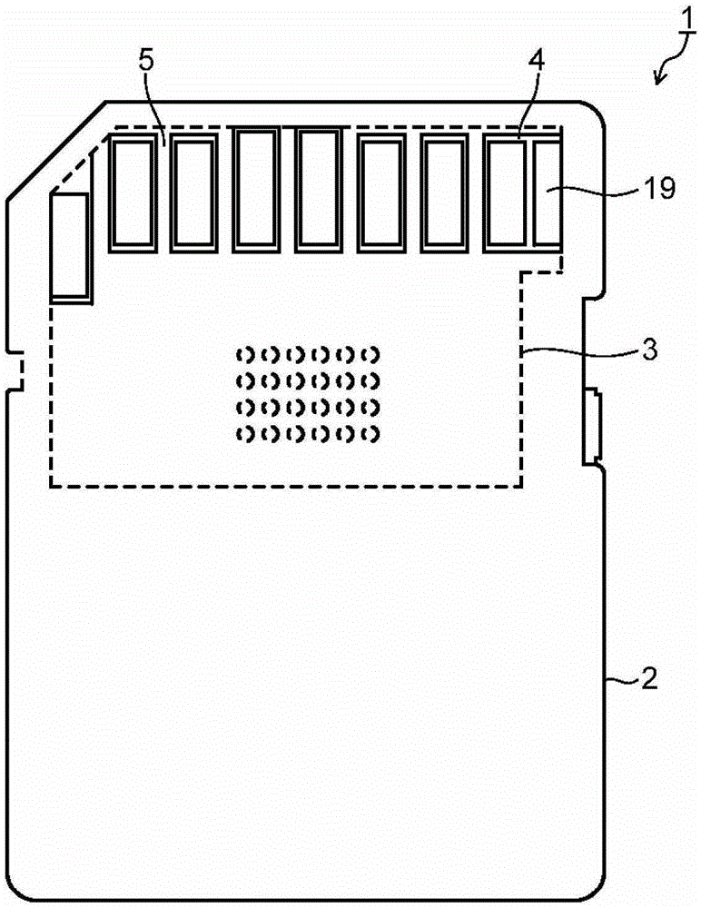
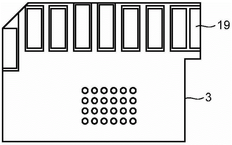
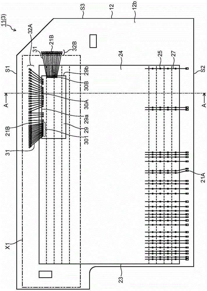
[0022] For the SiP-structure semiconductor memory device of the first embodiment, refer to Figure 3 to Figure 6 to illustrate. image 3 is a top perspective view showing the semiconductor memory device according to the first embodiment, Figure 4 is along image 3 A sectional view of the A-A line, Figure 5 yes image 3 It is a perspective view of the terminal formation surface of the wiring substrate in the semiconductor storage device seen from the upper surface (molding surface) of the semiconductor storage device, Figure 6 It is viewed from the perspective of the upper surface (molding surface) of the semiconductor memory device image 3 A perspective view of the chip mounting surface of the wiring substrate in the shown semiconductor memory device. The semiconductor storage device 11 ( 3 ) shown in these figures includes a wiring board 12 serving also as a substrate for forming external connection terminals and a substrate for mounting semiconductor chips. The wir...
no. 2 Embodiment approach )
[0048] Next, regarding the semiconductor memory device having the SiP structure of the second embodiment, refer to Figure 8 to Figure 11 Be explained. Figure 8 It is a top perspective view showing the semiconductor memory device of the second embodiment, Figure 9 is along Figure 8 A sectional view of the A-A line, Figure 10 It is viewed from the upper surface (molding surface) of the semiconductor memory device Figure 8 A perspective view seen from the terminal forming surface of the wiring substrate of the semiconductor memory device shown, Figure 11 It is viewed from the upper surface (molding surface) of the semiconductor memory device Figure 8 It is a perspective view seen from the chip mounting surface of the wiring board of the semiconductor memory device shown. In addition, the same code|symbol is attached|subjected to the same part as 1st Embodiment, and the description is abbreviate|omitted partly.
[0049] Figure 8 to Figure 11 The shown semiconductor...
PUM
 Abstract
Description
Claims
Application Information
 - R&D
- Intellectual Property
- Life Sciences
- Materials
- Tech Scout
- Unparalleled Data Quality
- Higher Quality Content
- 60% Fewer Hallucinations
Browse by: Latest US Patents, China's latest patents, Technical Efficacy Thesaurus, Application Domain, Technology Topic, Popular Technical Reports.
© 2025 PatSnap. All rights reserved.Legal|Privacy policy|Modern Slavery Act Transparency Statement|Sitemap|About US| Contact US: help@patsnap.com