Encapsulating method for LED chips

A LED chip and chip packaging technology, applied in the direction of electrical components, circuits, semiconductor devices, etc., can solve the problems of large volume, poor heat dissipation effect of LED chips, and poor firmness

Inactive Publication Date: 2013-09-11
SHANGHAI JIUJUN ELECTRONICS SCI & TECH
View PDF3 Cites 6 Cited by
  • Summary
  • Abstract
  • Description
  • Claims
  • Application Information

AI Technical Summary

Problems solved by technology

In this way, the heat dissipation effect of the LED chip will become relatively poor, and the firmness will not be good.
It will also cause light loss of the LED chip, which will gradually d

Method used


Image

  • Encapsulating method for LED chips

Examples


Embodiment Construction

[0013] The present invention will be further described below in conjunction with drawings and embodiments.

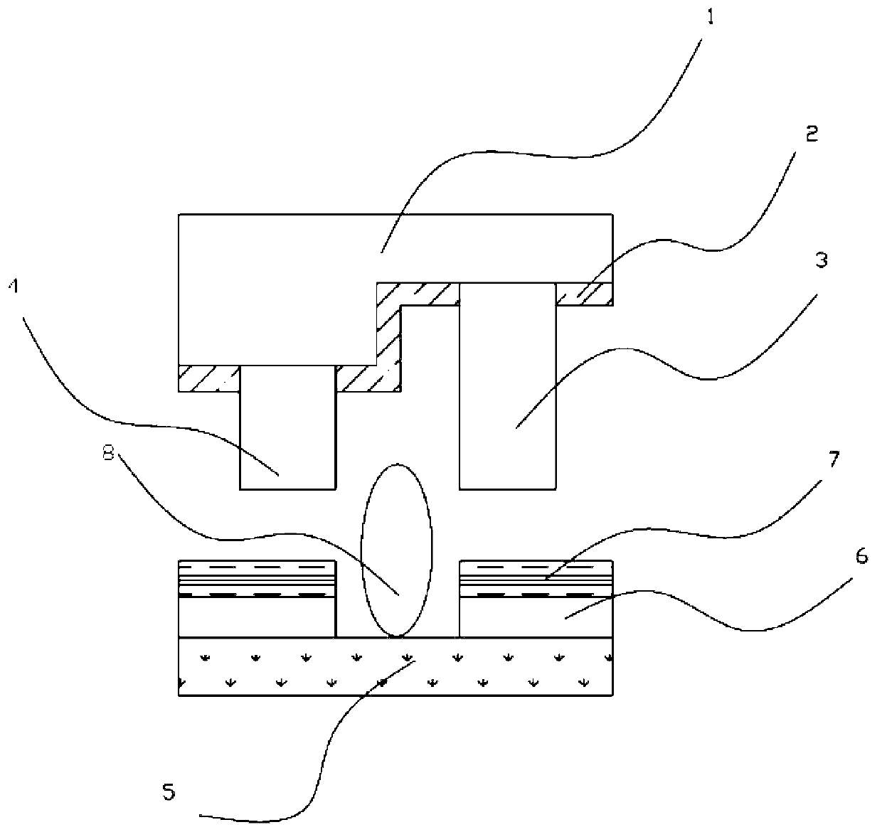
[0014] Such as figure 1 A LED chip packaging method is shown. The LED chip includes a substrate 1 , an insulating layer 2 , a P pole 3 and an N pole 4 . The insulating layer 2 , the P pole 3 and the N pole 4 are all arranged on one side of the substrate 1 , and the insulating layer 2 is laid on the substrate 1 except the P pole 3 and the N pole 4 . The material of the insulating layer 2 can be silicon dioxide. The thickness of the insulating layer 2 is between 4000 angstroms and 10000 angstroms. In this way, when the LED chip is heated and pressurized, the insulating layer 2 is not easily broken, and the insulating effect is better. Make short circuit between P pole 3 and N pole 4 difficult.

[0015] Tin 7 is added to the surface of the electrode 6 of the circuit board substrate 5 .

[0016] Glue 8 is provided on the upper surface of the circuit board substrate 5 ...


PUM

PropertyMeasurementUnit
Thicknessaaaaaaaaaa
Heightaaaaaaaaaa
Heightaaaaaaaaaa

Abstract

The invention discloses an encapsulating method for LED chips. Firstly, tin is added on the surfaces of electrodes of a circuit board substrate, and then glue is arranged on the part, except the electrodes, of the upper surface of the circuit board substrate, an LED chip is arranged on the circuit board substrate, the salient point of the P electrode and the salient point of the N electrode correspond to the electrodes on the circuit board substrate, and the LED chip is heated and pressurized to enable the salient point of the P electrode and the salient point of the N electrode to be connected with the tin on the electrodes of the circuit board substrate in an eutectic melting mode. When the LED chip is heated, the glue is solidified to enable the LED chip to be fixedly connected with the circuit board substrate. Hereto, the encapsulation of the LED chip is completed. The encapsulating method for the LED chips is simple in technology, firm in connection between the LED chip and the circuit board substrate, and not prone to falling off.

Description

technical field [0001] The invention belongs to the field of packaging of light-emitting diodes (LEDs), and more specifically relates to a packaging method of LED chips. Background technique [0002] The packaging method of the LED chip currently used is: the LED chip and the printed circuit board (PCB) substrate are conducted and packaged in a way of bonding metal wires. Since the metal wire is easy to break, it needs to be protected with glue. In this way, the heat dissipation effect of the LED chip will become relatively poor, and the firmness is not good. It will also cause light loss of the LED chip, so that the LED chip will gradually become darker during use, seriously affecting the quality and service life of the LED chip. Moreover, LED chips on the market are relatively large in size and high in cost. Contents of the invention [0003] The purpose of the present invention is to provide an improved LED chip packaging method. [0004] According to one aspect of ...

Claims


Application Information

Patent Timeline
IPC IPC(8): H01L33/00H01L33/48H01L33/62H01L33/56
Inventor 傅华贵
Owner SHANGHAI JIUJUN ELECTRONICS SCI & TECH
Why Eureka
Try Eureka