Liquid crystal display device, manufacturing method of the same and electronic equipment

A liquid crystal display device, liquid crystal layer technology, applied in chemical instruments and methods, devices for capturing or killing insects, transportation and packaging, etc., can solve problems such as light leakage

Active Publication Date: 2013-09-18
JAPAN DISPLAY INC
View PDF9 Cites 19 Cited by
  • Summary
  • Abstract
  • Description
  • Claims
  • Application Information

AI Technical Summary

Problems solved by technology

This may cause leakage of light

Method used


Image

  • Liquid crystal display device, manufacturing method of the same and electronic equipment
  • Liquid crystal display device, manufacturing method of the same and electronic equipment
  • Liquid crystal display device, manufacturing method of the same and electronic equipment

Examples


no. 1 example

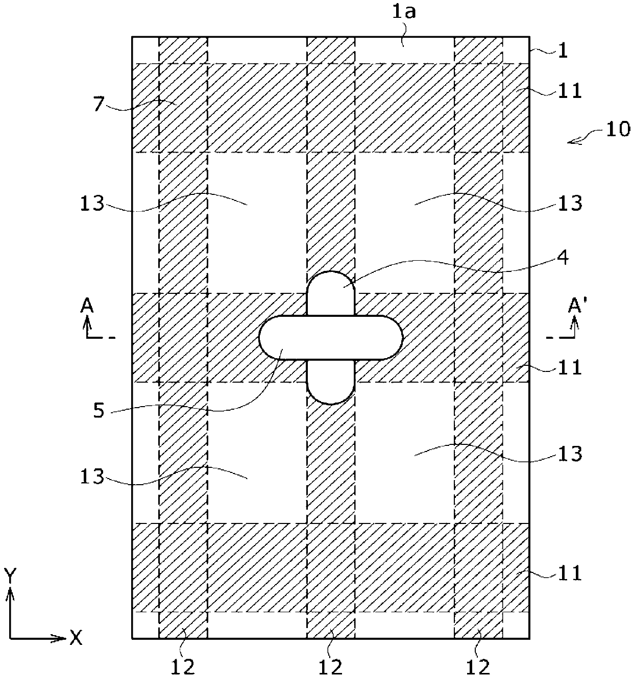
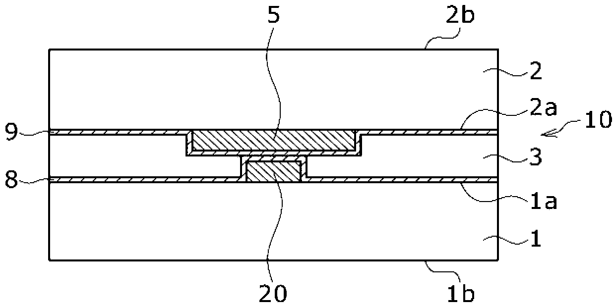
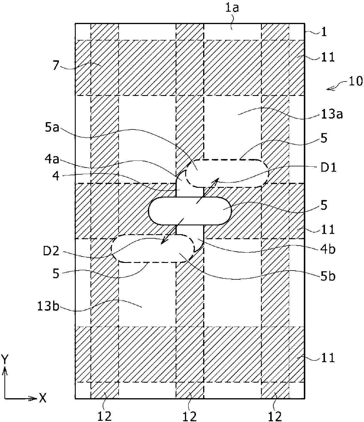
[0036] Figure 1A and 1B is a schematic diagram showing an example of the liquid crystal display device according to the first embodiment. Figure 1A shows a top view of the liquid crystal display device 10, and Figure 1B shows along the Figure 1A A cross-sectional view taken along line A-A'. It should be noted Figure 1A The top view of FIG. 2 does not show the counter substrate 2 and the liquid crystal layer 3 .

[0037] The liquid crystal display device 10 includes an array substrate 1 , a counter substrate 2 , a liquid crystal layer 3 , a spacer portion 4 and a spacer portion 5 , and alignment films 8 and 9 .

[0038] The array substrate 1 has, for example, a plurality of pixel regions arranged in a matrix. A TFT (Thin Film Transistor) and a pixel electrode are formed in each of the pixel regions. For example, a transparent glass substrate is used as the array substrate 1 .

[0039] In addition, the array substrate 1 has a surface 1a and a surface 1b on the opposite ...

no. 2 example

[0056] Next, a second embodiment will be described.

[0057] image 3 is a plan view showing the liquid crystal display device according to the second embodiment. Figure 4 is a partially enlarged view of the spacer part and its surrounding area. Figure 5 is along image 3 A cross-sectional view taken along line B-B' in . It should be noted image 3 Not only components other than the spacer portion 74 of the counter substrate 30 but also the pixel electrode 68 are not shown in .

[0058] The liquid crystal display device 100 includes an array substrate 20 , an opposite substrate 30 and a liquid crystal layer 40 . In the liquid crystal display device 100 , the pixel electrodes 68 are formed on the array substrate 20 , and the common electrodes 73 are formed on the opposite substrate 30 . The liquid crystal display device is a liquid crystal display device of TN (twisted nematic) mode, VA (vertical alignment) mode, and ECB (electrically controlled birefringence) mode.

...

example 1)

[0103] Next, a modified example of the second embodiment is described as Modified Example 1. FIG.

[0104] Figure 8 is a sectional view showing Modified Example 1.

[0105] The liquid crystal display device 110 differs from the liquid crystal display device 100 in that the spacer portion 81 is formed instead of the spacer portion 67 . The liquid crystal display device 110 is the same as the liquid crystal display device 100 in all other respects. The spacer portion 81 is made of, for example, acrylic resin. It should be noted that the spacer portion 81 is the same as the spacer portion 67 in shape and arrangement.

[0106] That is, in the liquid crystal display device 100 , the spacer portion 67 is formed with a part of the organic insulating film 66 . However, in the liquid crystal display device 110 , the spacer portion 81 is formed separately from the organic insulating film 66 . For example, this configuration makes it possible to select a material that is more resis...


PUM


Abstract

Provided are a liquid crystal display device, a manufacturing method of the same and electronic equipment. The liquid crystal display device includes first and second substrates, liquid crystal layer, and first and second spacer sections. The first substrate has a first surface including a light-shielding region in a lattice form and a plurality of opening regions surrounded by the light-shielding region. The light-shielding region includes a plurality of first extended portions extending in a first direction and a plurality of second extended portions extending in a second direction that intersects the first direction. The first substrate has a plurality of transistors formed thereon. The second substrate has a second surface that is opposed to and spaced from the first surface. The liquid crystal layer is arranged between the first and second surfaces. The first spacer section has long sides oriented in the second direction, and the second spacer section has long sides oriented in the first direction. The spacer sections protrude into the liquid crystal layer.

Description

technical field [0001] The present disclosure relates to a liquid crystal display device for displaying images, a method of manufacturing the liquid crystal display device, and electronic equipment having the liquid crystal display device. Background technique [0002] There is a type of liquid crystal display device that includes an array substrate, a counter substrate, and a liquid crystal layer. The array substrate has transistors formed in each of a plurality of pixel regions arranged in a matrix. The opposite substrate is disposed opposite to the array substrate. A liquid crystal layer is formed between the array substrate and the opposite substrate. Each of the pixel areas includes an opening area for passing light and a light shielding area surrounding the opening area. [0003] In such a liquid crystal display device, for example, an electric field based on image data is supplied to a liquid crystal layer from a pixel electrode and a common electrode for each pixe...

Claims


Application Information

Patent Timeline
Patent Type & Authority Applications(China)
IPC IPC(8): G02F1/1339G02F1/1333
CPCG02F2201/503G02F1/13394G02F1/13396A01M7/0082Y10S43/90B01F35/50G02F1/1339G02F1/136295G02F1/133512
Inventor 野村盛一
Owner JAPAN DISPLAY INC
Why Eureka
Try Eureka