Write processing method and device for phase change memory

A technology of phase change memory and processing method, which is applied in the field of write processing method and device of phase change memory, and can solve the problems of increasing the switching time delay of reading and writing data, shortening the switching time of reading and writing data, and not being suitable for synchronous interface phase change memory, etc. , to achieve the effect of saving read-write switching delay, solving application limitations, and shortening switching time

Active Publication Date: 2017-02-01
HUAWEI TECH CO LTD
View PDF2 Cites 0 Cited by
  • Summary
  • Abstract
  • Description
  • Claims
  • Application Information

AI Technical Summary

Problems solved by technology

However, in this method, since the read and compare operations are performed before the data is written, and then the write pulse is output to start the write operation, the separation of the read and write operations increases the delay in the switching time of the read and write data.
[0004] In the second method, when the address of the phase change memory is sent first and the data has not been sent, the data is read from the corresponding address of the phase change memory in advance, and the data is directly compared when the data is sent. If the read data and If the data to be written is the same, the current write operation is abandoned, otherwise the write operation is performed. Although this method can shorten the switching time of reading and writing data, this method is only applicable to the phase change memory of the asynchronous interface, not suitable for the synchronous interface phase change memory, there are application limitations

Method used


Image

  • Write processing method and device for phase change memory
  • Write processing method and device for phase change memory
  • Write processing method and device for phase change memory

Examples


Embodiment Construction

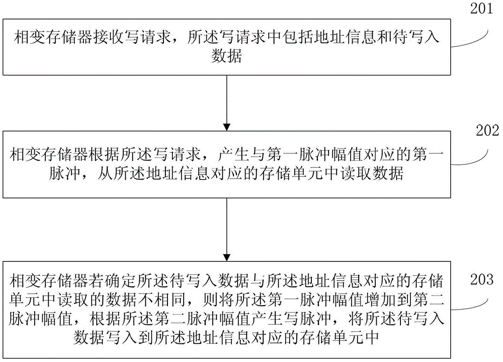
[0039] In order to make the purpose, technical solutions and advantages of the embodiments of the present invention clearer, the technical solutions in the embodiments of the present invention will be clearly and completely described below in conjunction with the drawings in the embodiments of the present invention. Obviously, the described embodiments It is a part of embodiments of the present invention, but not all embodiments. Based on the embodiments of the present invention, all other embodiments obtained by persons of ordinary skill in the art without creative efforts fall within the protection scope of the present invention.

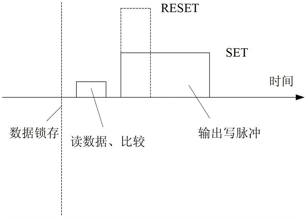
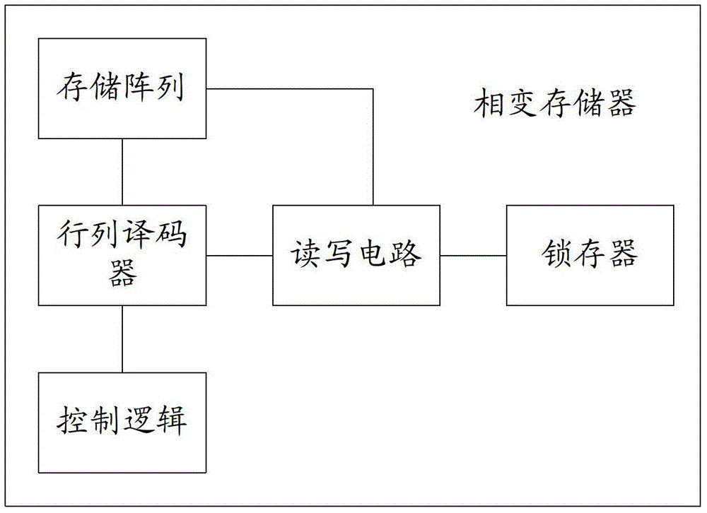
[0040] The phase change memory described in the embodiment of the present invention includes a phase change memory with an asynchronous interface and a phase change memory with a synchronous interface, wherein the asynchronous interface is similar to the interface of a Static Random Access Memory (SRAM), and the synchronous interface is similar to ...


PUM


Abstract

The invention discloses a write processing method and a device of a phase change memorizer. The method comprises the steps that when the phase change memorizer receives a write request, a first pulse corresponding to a first pulse amplitude is generated according to the write request; data is read from a memory cell corresponding to address information included in the write request; if to-be-written data included in the write request is different from the read data, the first pulse amplitude is increased to a second pulse amplitude; a write pulse is generated according to the second pulse amplitude; and the to-be-written data is written into the memory cell corresponding to the address information. The time required by increasing the first pulse amplitude to the second pulse amplitude is relatively short, so that the switching time from data reading to data writing is greatly shortened, and the data reading and the data writing can be accomplished simultaneously; the method can be applied to the phase change memorizer with a synchronous interface and the phase change memorizer with an asynchronous interface; and the application performance of the phase change memorizer is improved.

Description

technical field [0001] Embodiments of the present invention relate to the field of communication technologies, and in particular, to a write processing method and device for a phase change memory. Background technique [0002] Phase change memory is a new type of semiconductor memory that stores information through different states of phase change materials. When phase change memory performs a write operation, if the data to be written is the same as the existing data in the storage unit, it will still be executed again. In the writing process, the phase change material is heated once by generating a writing pulse. Therefore, as the number of times of writing increases, the loss of the phase change material will be caused, and its resistance value will deviate from the rated range, making it impossible to continue programming, thus causing the failure of the memory cell. [0003] In order to solve the loss problem of the phase change memory, in the first method, before perf...

Claims


Application Information

Patent Timeline
Patent Type & Authority Patents(China)
IPC IPC(8): G11C13/00
Inventor 李延松
Owner HUAWEI TECH CO LTD
Why Eureka
Try Eureka