

Crystalline silicon solar cell and method for manufacturing same
A technology of solar cells and crystalline silicon, applied in circuits, photovoltaic power generation, electrical components, etc., can solve the problems of reduced conversion efficiency of cells, increased costs, and increased refractive index of silicon nitride films, etc.
- Summary
- Abstract
- Description
- Claims
- Application Information
AI Technical Summary
Problems solved by technology
Method used
Image

Examples
Embodiment 1
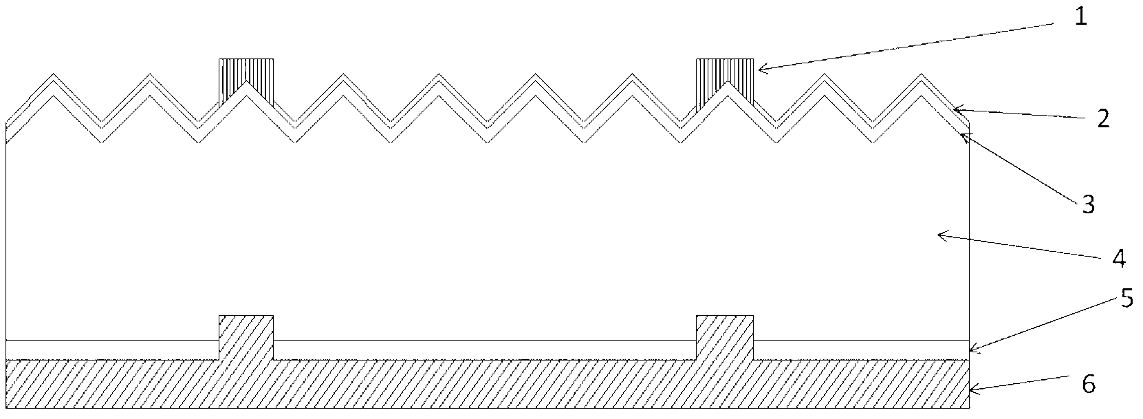
[0037] Using a P-type monocrystalline silicon wafer as the base material (that is, the aforementioned substrate), the specific steps of the manufacturing method are as follows:
[0038] (1) P-type silicon wafers are damaged and textured, and cleaned;
[0039] (2) Tubular phosphorus diffusion, diffusion resistance 60ohm / sq;
[0040] (3) Wet edge cutting, and remove the PN junction on the back;
[0041] (4) Using HNO3 with a mass concentration of 69%, at 70°C for 10 minutes, grow a layer of silicon oxide on the upper surface of the silicon wafer with a thickness of 1-100nm (preferably 3-8nm);
[0042] (5) A silicon nitride film (as an anti-reflection film) is grown on the upper surface of silicon oxide by PECVD, with a thickness of 40-150nm (preferably 75nm);
[0043] (6) Print electrodes, sinter and test sorting;
[0044] (7) String welding battery slices;
[0045] (8) Laying, laminating, junction boxes, framing, and making finished components.
[0046] The solar cells are...
Embodiment 2
[0048] Using a P-type monocrystalline silicon wafer as the base material (that is, the aforementioned substrate), the specific steps of the manufacturing method are as follows:
[0049] (1) P-type silicon wafers are damaged and textured, and cleaned;
[0050] (2) Tubular phosphorus diffusion, diffusion resistance 60ohm / sq;
[0051] (3) Wet edge cutting, and remove the PN junction on the back;
[0052] (4) A layer of silicon oxide film is grown on the upper surface of the silicon wafer by PECVD, with a thickness of 10nm;
[0053] (5) A silicon nitride film (as an anti-reflection film) is grown on the upper surface of the silicon oxide film by PECVD, with a thickness of 70nm;
[0054] (6) Print electrodes, sinter and test sorting;
[0055] (7) String welding battery slices;
[0056] (8) Laying, laminating, junction boxes, framing, and making finished components.
[0057] The solar cells are made into modules, and the module materials are made of conventional commercial modu...
Embodiment 3
[0059] Using a P-type monocrystalline silicon wafer as the base material (that is, the aforementioned substrate), the specific steps of the manufacturing method are as follows:
[0060] (1) P-type silicon wafers are damaged and textured, and cleaned;
[0061] (2) Tubular phosphorus diffusion, diffusion resistance 60ohm / sq;
[0062] (3) Wet edge cutting, and remove the PN junction on the back;
[0063] (4) Using PECVD to grow a layer of amorphous silicon film on the upper surface of the silicon wafer with a thickness of 1-50nm (preferably 3-5nm);
[0064] (5) A silicon nitride film (as an anti-reflection film) is grown on the upper surface of silicon oxide by PECVD method, with a thickness of 75nm;
[0065] (6) Print electrodes, sinter and test sorting;
[0066] (7) String welding battery slices;
[0067] (8) Laying, laminating, junction boxes, framing, and making finished components.
[0068]The solar cells are made into modules, and the module materials are made of conve...
PUM
| Property | Measurement | Unit |
|---|---|---|
| thickness | aaaaa | aaaaa |
| thickness | aaaaa | aaaaa |
| thickness | aaaaa | aaaaa |
Abstract
Description
Claims
Application Information