Circuit board and manufacturing method thereof

A production method and circuit board technology, applied in the directions of printed circuit components, secondary processing of printed circuits, and non-metallic protective layer coating, etc., can solve the problem of poor adhesion of cover films, easy oxidation, and inability to effectively protect circuits, etc. question

Active Publication Date: 2013-09-25
HONGQISHENG PRECISION ELECTRONICS (QINHUANGDAO) CO LTD +1
View PDF4 Cites 8 Cited by
  • Summary
  • Abstract
  • Description
  • Claims
  • Application Information

AI Technical Summary

Problems solved by technology

However, in the bonding process, it is very easy to generate air bubbles between the cover film and the circuit, which will make the bonding effect of the cover film poor, not only make the circuit unable to be effectively protected and easy to oxidize, but also increase the risk of explosion in the subsequent process. The danger of the board, and also affect the appearance of the circuit board product
In other words, poor lamination of the cover film will lead to a decrease in the quality of the circuit board product

Method used


Image

  • Circuit board and manufacturing method thereof
  • Circuit board and manufacturing method thereof
  • Circuit board and manufacturing method thereof

Examples


Embodiment Construction

[0031] The manufacturing method of the circuit board provided by the technical solution and the produced circuit board will be further described in detail below in conjunction with the accompanying drawings and embodiments.

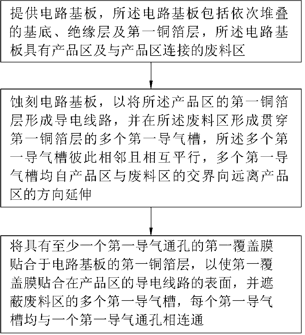
[0032] see figure 1 , the manufacturing method of the circuit board provided by the technical solution, comprising steps:

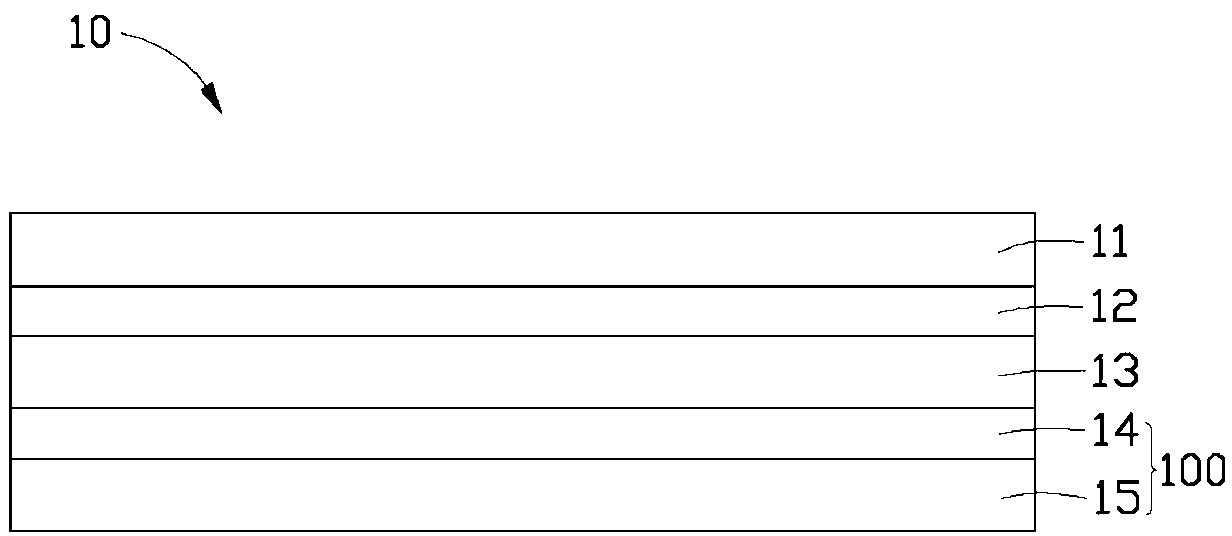
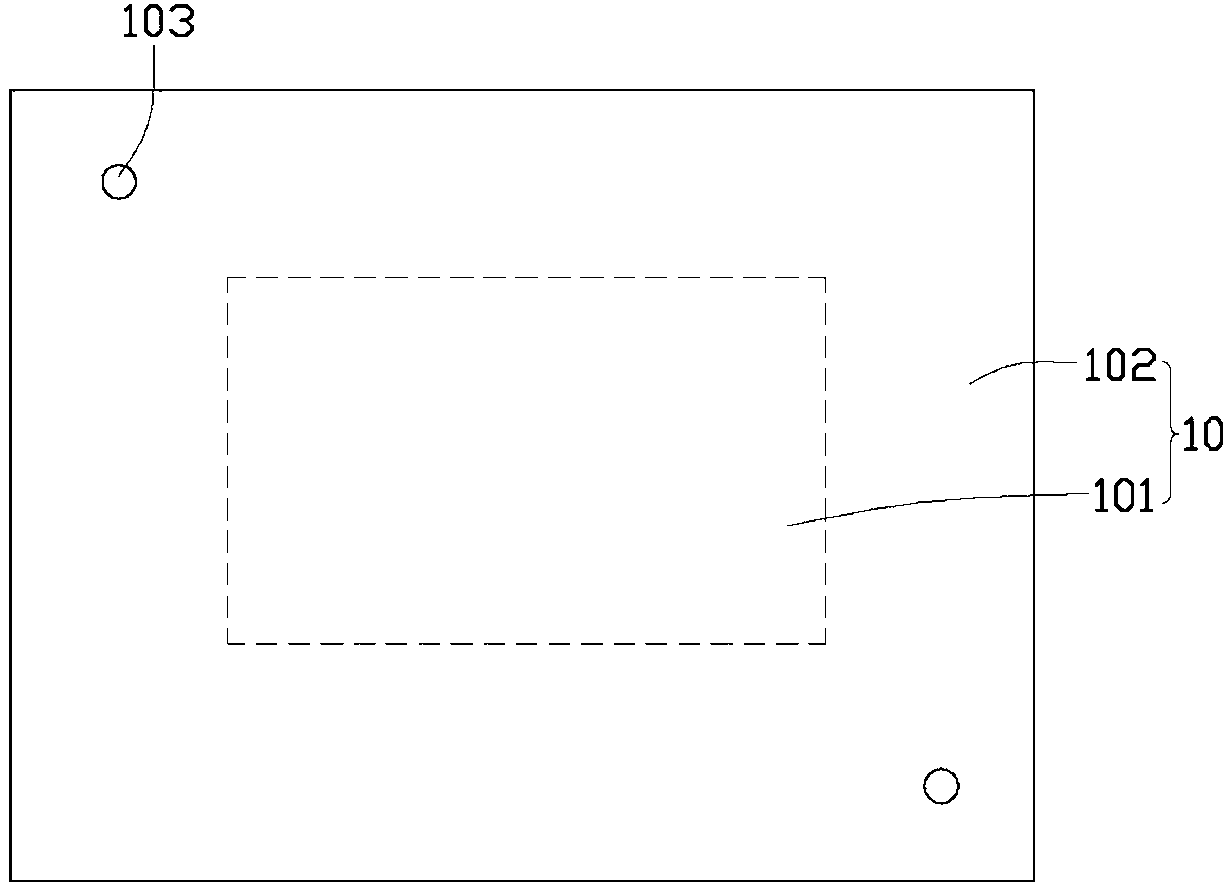
[0033] For a first step, see figure 2 and image 3 , providing a circuit substrate 10 . In this embodiment, the circuit substrate 10 is a double-sided adhesive flexible copper clad laminate, which includes a first copper foil layer 11, a first adhesive layer 12, an insulating layer 13, a second The adhesive layer 14 and the second copper foil layer 15 . The insulating layer 13 plays a supporting role, and its most commonly used material is polyimide (Polyimide, PI), but it can also be polyethylene terephthalate (Polyethylene Terephtalate, PET) or polyethylene naphthalate. Poly(ethylene naphthalate), PEN. The second adhesive la...


PUM

PropertyMeasurementUnit
Widthaaaaaaaaaa

Abstract

The invention provides a manufacturing method of a circuit board. The manufacturing method of the circuit board comprises the steps that a circuit substrate with a product zone and a waste zone is offered and the circuit substrate comprises a substrate body, an insulating layer and a copper foil layer which are sequentially stacked; the circuit substrate is etched, so that an electricity conductive circuit is formed on the copper foil layer of the product zone, a plurality of air guiding grooves penetrating through the copper foil layer are formed in the waste zone, the air guiding grooves are mutually adjacent and mutually parallel and extend in the direction far away from the product zone from a border of the product zone and the waste zone; a covering film provided with at least one air guiding through hole is attached to the copper foil layer, so that the covering film is attached to the surface of the electricity conductive circuit and covers the air guiding grooves, and each air guiding groove is communicated with one air guiding through hole. The invention further provides the circuit board manufactured through the manufacturing method.

Description

technical field [0001] The invention relates to circuit board technology, in particular to a circuit board with better product quality and a manufacturing method thereof. Background technique [0002] With the advancement of science and technology, circuit boards are widely used in electronic products. For the application of the circuit board, please refer to the literature Takahashi, A. Ooki, N. Nagai, A. Akahoshi, H. Mukoh, A. Wajima, M. Res. Lab, High density multilayer printed circuit board for HITAC M-880, IEEE Trans . on Components, Packaging, and Manufacturing Technology, 1992, 15(4): 418-425. [0003] The circuit on the surface of the circuit board is generally protected by a cover film, and the cover film is generally attached to the circuit surface by pressing. However, in the bonding process, it is very easy to generate air bubbles between the cover film and the circuit, which will make the bonding effect of the cover film poor, not only make the circuit unable ...

Claims


Application Information

Patent Timeline
IPC IPC(8): H05K3/28H05K1/02
Inventor 杨树平孔全伟黄海刚
Owner HONGQISHENG PRECISION ELECTRONICS (QINHUANGDAO) CO LTD
Why Eureka
Try Eureka