Method for customizing wiring in integrated circuit

A technology for custom wiring and integrated circuits, applied in circuits, electrical components, electro-solid devices, etc., which can solve problems such as heavy workload for engineers, prolonged project time, and impact on project progress.

Active Publication Date: 2013-10-23
KTMICRO ELECTRONICS
View PDF6 Cites 3 Cited by
  • Summary
  • Abstract
  • Description
  • Claims
  • Application Information

AI Technical Summary

Problems solved by technology

[0005] Since the back-end design is a process of repeated iterations, if engineers have to perform multiple manual operations during each iteration, it will prolong the project time
Moreover, automated tools are likely to change the position of the above-mentioned units, change the position of the above-mentioned lines, or delete or add new lines during the subsequent optimization process; if the engineer prohibits the automation tool from doing Any modification, then, will reduce the optimization level of the automated tool
Furthermore, if there are a large number of wirings with special requirements, the workload of engineers will be huge, which will seriously affect the progress of the project and further affect the optimization ability of automation tools

Method used


Image

  • Method for customizing wiring in integrated circuit
  • Method for customizing wiring in integrated circuit
  • Method for customizing wiring in integrated circuit

Examples


Embodiment Construction

[0024] The present invention will be further described below in conjunction with the accompanying drawings and specific embodiments.

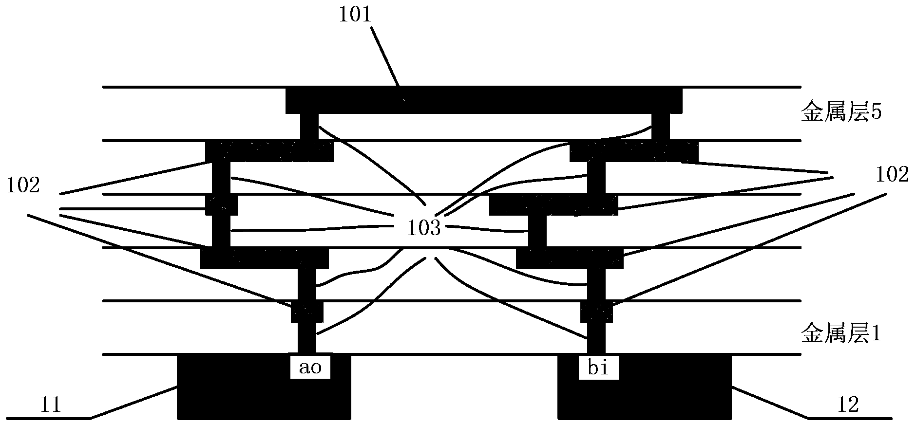
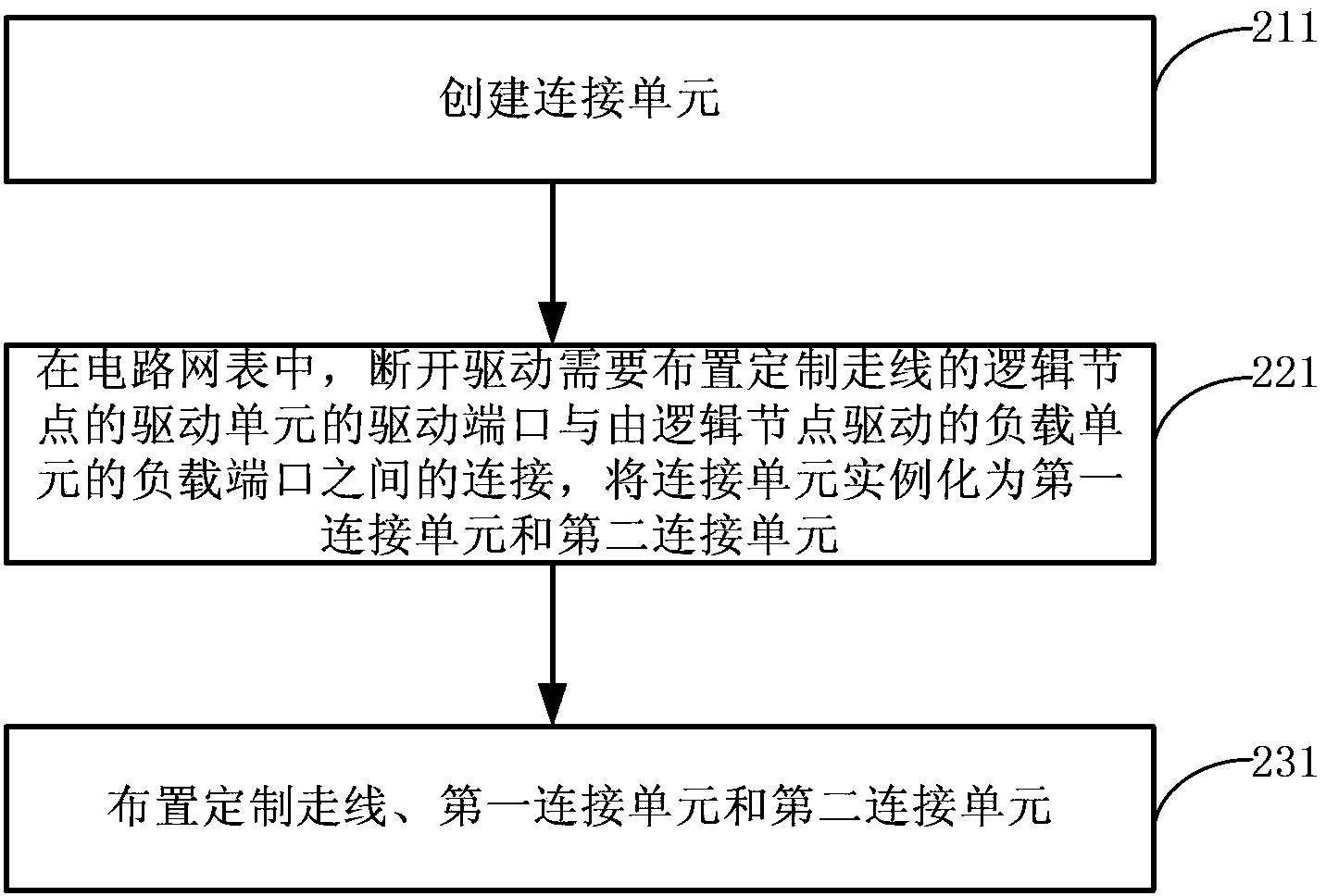
[0025] Such as figure 2 As shown, it is a schematic flow chart of an embodiment of a method for implementing custom wiring in an integrated circuit according to the present invention, including the following steps:

[0026] Step 211, creating a connection unit;

[0027] Wherein, the connection unit has at least one input port and at least one output port, and the input port is connected to the output port. In this case, the logic of the input port and the output port are the same; in this step, the layout file of the connection unit is also created, including the connection unit. The pattern and size of each mask layer, the position of the input port and the position of the output port are defined on the layout; optionally, in step 211, the input port and the output port of the connection unit can be located in the same connection layer or in...


PUM


Abstract

The invention relates to a method for customizing wiring in an integrated circuit. The method comprises the following steps: creating a connection unit; disconnecting the connection between a drive port of a drive unit for driving a logic node requiring distribution of a customized wire and a load port of a load unit driven by the logic node, instantiating the connection unit into a first connection unit and a second connection unit; distributing the customized wire, the first connection unit and the second connection unit, wherein one end of the customized wire is in contact with an output port of the first connection unit, and the other end of the customized wire is in contact with an input port of the second connection unit. The method achieves customized wiring, meanwhile, the workload of manual operation of design staff is greatly reduced, and the optimization of locating and wiring by an automated tool is not affected.

Description

technical field [0001] The invention relates to the field of integrated circuits, in particular to a method for realizing customized routing in an integrated circuit. Background technique [0002] The design automation of large-scale integrated circuits has been developed for many years. Integrated circuit automation tools can automatically handle some back-end work such as chip layout and routing, reducing manual intervention. However, as the scale of integrated circuits becomes larger and more and more modules are integrated in a system on a chip (System On a Chip, SOC for short), the back-end design work of integrated circuits becomes more and more complicated. In order to meet performance, area, or other special requirements, back-end designers have to manually handle the layout and routing of some locations according to special requirements, for example: requiring a group of traces to be placed in a certain channel, or requiring a group of traces to It is arranged in a...

Claims


Application Information

Patent Timeline
Patent Type & Authority Applications(China)
IPC IPC(8): G06F17/50H01L27/02
Inventor 陈世柱谭洪贺邓思园
Owner KTMICRO ELECTRONICS
Why Eureka
Try Eureka