Test method and device for gate oxide layer trap density and position

A test method and trap density technology, applied in the direction of semiconductor/solid-state device test/measurement, etc., can solve the problems of not considering the trap density of pn junction and the lack of trap density test.

Active Publication Date: 2015-10-07
PEKING UNIV
View PDF7 Cites 0 Cited by
  • Summary
  • Abstract
  • Description
  • Claims
  • Application Information

AI Technical Summary

Problems solved by technology

[0004] However, the above-mentioned test methods only focus on the density of traps on the gate oxide layer interface of n-type and p-type MOS devices, and lack of density testing of traps near the interface, especially without taking into account the trap density of pn junctions and pn junction traps. The location distribution of

Method used


Image

  • Test method and device for gate oxide layer trap density and position
  • Test method and device for gate oxide layer trap density and position
  • Test method and device for gate oxide layer trap density and position

Examples


Embodiment 1

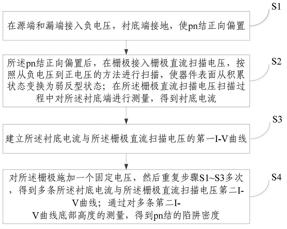
[0041] Such as figure 1 As shown, a method for testing gate oxide trap density and position includes the following steps:

[0042] S1, a negative voltage is connected to the source and drain terminals, the substrate terminal is grounded, and the pn junction is forward biased;

[0043] S2. After the pn junction is forward biased, the gate DC scan voltage is connected to the gate, and the scan is performed from negative voltage to positive voltage, so that the surface of the device is transformed from an accumulation state to a weak inversion state; Measuring the substrate end during the gate DC scanning voltage scanning process to obtain the substrate current;

[0044] S3. Establish a first I-V curve of the substrate current and the gate DC scan voltage;

[0045] S4. Apply a fixed voltage to the gate, and then repeat steps S1 to S3 multiple times to obtain a plurality of second IV curves of the substrate current and the gate DC scanning voltage; by comparing the plurality of second IV ...

Embodiment 2

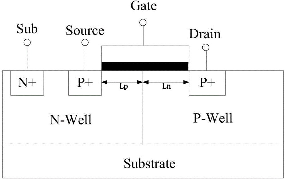
[0072] A gate oxide trap density and position test device, which is characterized by comprising an n-type MOSFET and a corresponding p-type gate oxide capacitor, or a p-type MOSFET and a corresponding n-type gate oxide capacitor; the n-type MOSFET and the corresponding n-type gate oxide capacitor The corresponding p-type gate oxide capacitance and the junction of the p-type MOSFET and its corresponding n-type gate oxide capacitance form a pn junction.

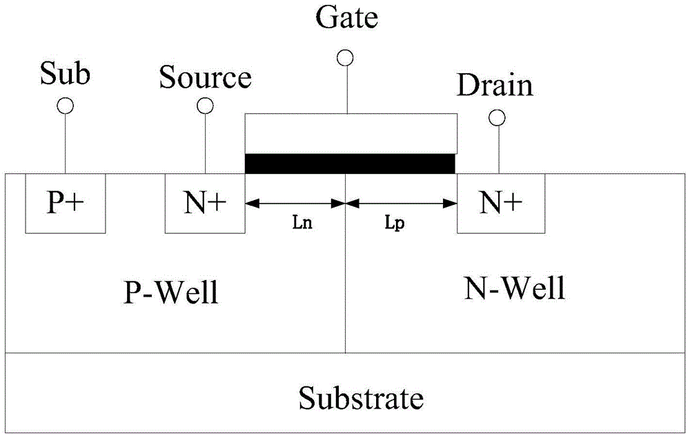
[0073] As shown in Figure 3(a), taking the n-type gate oxide interface trap density test device as an example, the left side of the n-type test device is the n-type MOSFET device part, and + , P-well and gate constitute the source, substrate and gate of the test device of the present invention. The right side of the test device is the p-type gate oxide capacitor part, which is composed of n + , N-well and gate constitute the drain, substrate and gate of the device of the present invention. The gate is shared, thus forming a gate o...


PUM


Abstract

The invention provides a method and a device for testing trap density and position of a gate oxide layer, and relates to the technical field of quality and reliability testing of an MOS (Metal Oxide Semiconductor) device. The method comprises the following steps: S1, accessing negative voltage at a source end and a drain end, grounding at a substrate end, so that p and n nodes are forward bias; S2, after the p and n nodes are forward bias, accessing a grid direct-current scanning voltage at a grid, and scanning from negative voltage to positive voltage, so that the surface of the device becomes weak inversion state from accumulation state; measuring the substrate end during the scanning process so as to obtain substrate current; S3, establishing a first I-V curve of the substrate current and the grid direct-current scanning voltage; S4, applying a fixed voltage to the grid, repeating the steps S1 to S 3 for multiple times so as to obtain a plurality of second I-V curves; measuring the heights of bottoms of the second I-V curves so as to obtain the trap density of p and n nodes. According to the method and the device, the strap density of the p and no nodes can be measured and the positions of traps can be positioned, so that the design of the device is improved so as to reduce the traps.

Description

Technical field [0001] The invention relates to the technical field of MOS device quality and reliability testing, in particular to a method and device for testing the density and position of gate oxide traps. Background technique [0002] With the rapid development of semiconductor technology and the substantial increase in the integration of microelectronic chips, the design and processing level of integrated circuits has entered the era of nano-MOS. As the core of MOS devices, the gate oxide layer plays an important role in the quality and reliability evaluation of MOS devices. Among them, the interface trap density of the gate oxide layer is one of the very important indicators. The generation of gate oxide layer interface traps reduces the mobility of the device, resulting in a decrease in device performance. Therefore, it is very necessary to monitor the gate oxide layer interface traps in the process flow. [0003] The commonly used gate oxide interface trap density test de...

Claims


Application Information

Patent Timeline
Patent Type & Authority Patents(China)
IPC IPC(8): H01L21/66
Inventor 何燕冬韦超张钢刚张兴
Owner PEKING UNIV
Why Eureka
Try Eureka